

Backside silicon wafer design reducing image artifacts from infrared radiation
- Summary
- Abstract
- Description
- Claims
- Application Information
AI Technical Summary
Benefits of technology
Problems solved by technology
Method used
Image

Examples
first embodiment
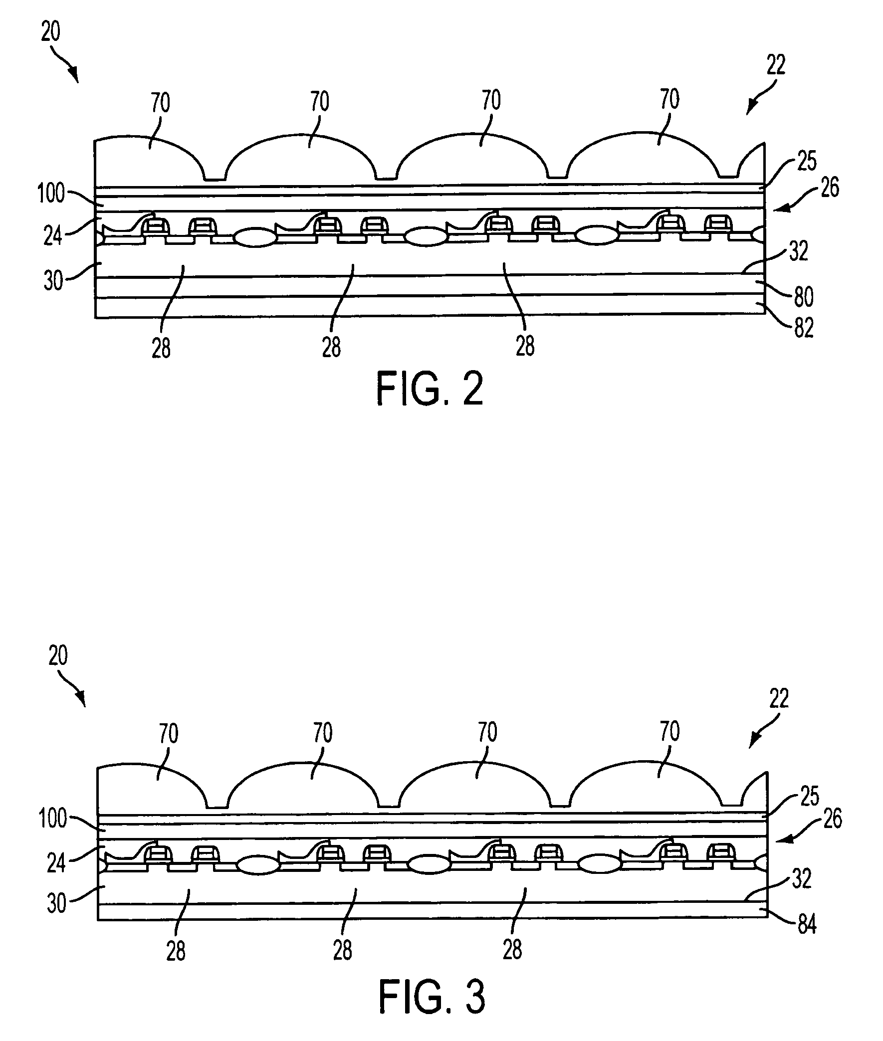
[0042] Referring now to the drawings, where like elements are designated by like reference numerals. Reference is now made to FIG. 2, which schematically shows a solid-state imager 20 according to the present invention. The imager 20 comprises a color filter layer 100 and a spacer layer 25 formed over a pixel cell array 26 as part of the same substrate 30, which may be any of the types of substrate described above. A micro-lens array 70 is formed over the color filter layer 100 and spacer layer 25. The pixel cell array 26 comprises a plurality of pixel sensor cells 28 formed in and over a first surface of the substrate 30, and is covered by a protective layer 24 which includes a passivation and planarization layer for the imager 20 as well as various metalization layers for connections. The passivation layer included in protective layer 24 may be a layer of BPSG, PSG, BSG, silicon dioxide, silicon nitride, polyimide, or other well-known light transmissive insulator. The metallizatio...
second embodiment
[0047] Reference is now made to FIG. 3 which schematically illustrates the solid-state imager 20 of the present invention. The illustrated FIG. 3 embodiment comprises a micro-lens array 70 formed over a color filter layer 100 and spacer layer 25, which are formed over a pixel cell array 26 formed in and / or over a first surface of substrate 30, which may be any of the types of substrate described above. The imager 20 further comprises an absorption layer 84 formed on a second surface 32 of the substrate 30. The absorption layer 84 may be formed of any suitable material which absorbs IR radiation at the wavelength of between about 800 to about 1150 nm. Preferably the absorption layer 84 is formed from Ge, SiGe, SiC, or the like. Most preferably, the absorption layer 84 is formed from germanium, as germanium for these purposes can be deposited on the surface of the substrate 30 using standard vacuum deposition techniques. While the absorption layer 84 is illustrated as a single layer, ...
third embodiment
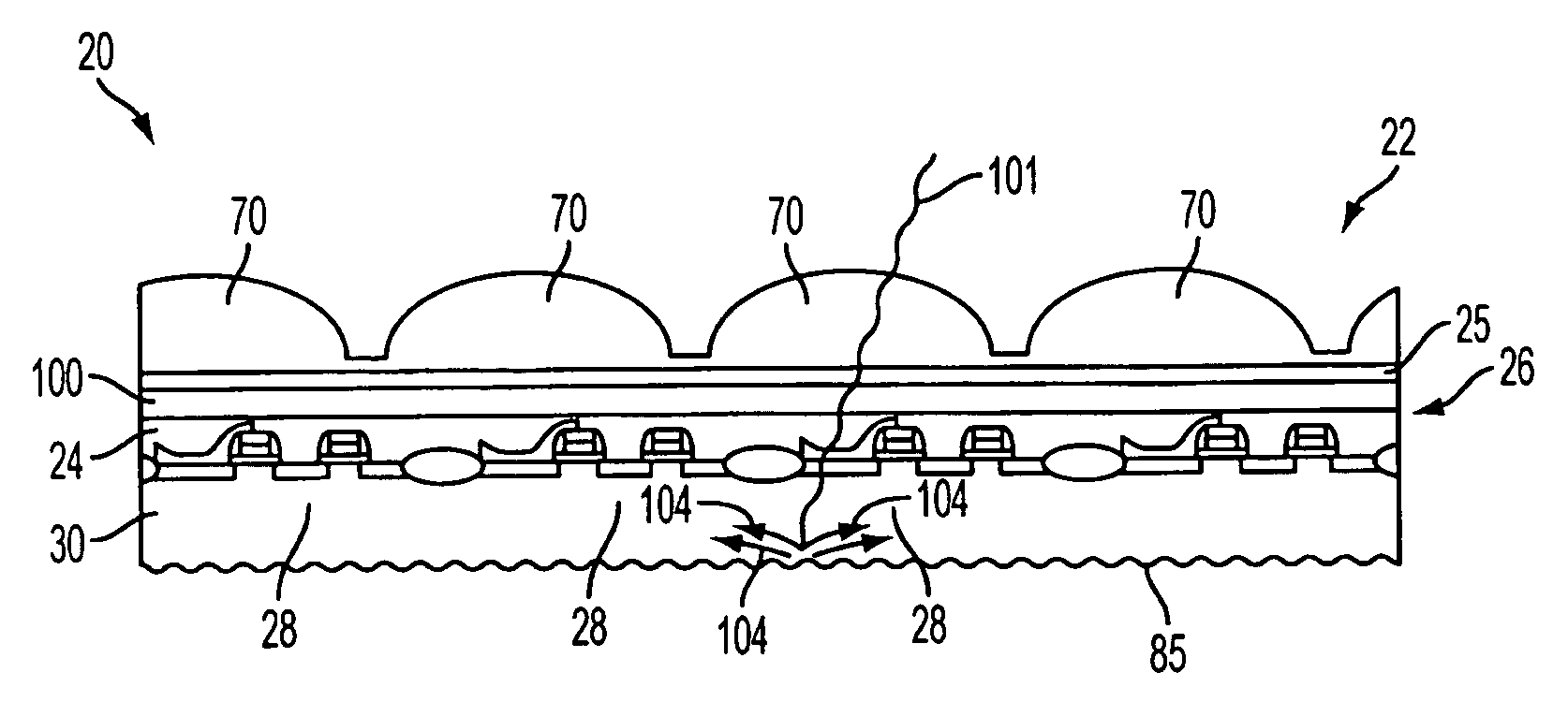
[0049] Reference is now made to FIG. 4, which schematically illustrates the solid-state imager 20 of the present invention. The illustrated embodiment comprises an imaging device having a micro-lens array 70 formed over a color filter layer 100 and spacer layer 25, which are formed over a pixel cell array 26 formed in and / or over a first surface of substrate 30. The imager 20 further comprises a roughened second substrate surface 85.
[0050] Roughening of the second substrate surface 85 in the perpendicular direction with respect to the second surface 32 provides the scattering of IR radiation instead of direct reflection to the dark pixels. Thus, the quantity of photons 101 hitting dark pixels can be reduced by scattering the photons 104 away from the dark pixels. FIG. 5 illustrates experimental results showing reducing of image artifacts from bright halogen lamp (row banding) with a roughened second surface 85 of the substrate 30. FIG. 5A is an image taken with an imaging device hav...
PUM
 Abstract
Description
Claims
Application Information