Chevron CMOS trigate structure

a tri-gate structure and cmos technology, applied in the field of chevron cmos tri-gate structure, can solve the problems of delay in the corresponding mosfet, and achieve the effects of reducing delay, reducing mobility, and optimizing mobility

Inactive Publication Date: 2007-02-15
ALSEPHINA INNOVATIONS INC
View PDF6 Cites 19 Cited by
  • Summary
  • Abstract
  • Description
  • Claims
  • Application Information

AI Technical Summary

Benefits of technology

[0007] The disclosure presents an improved structure for a chevron tri-gate MOSFET and a method of forming the structure. Generally, the structure comprises two different type chevron tri-gate MOSFETs (e.g., an n-FET and a p-FET) formed on the same substrate. Each MOSFET has a channel region in a semiconductor fin. The semiconductor fins have a non-orthogonal, non-parallel orientation with respect to each other and, thus, each semiconductor fin has essentially a different crystalline orientation. The different crystalline orientations ensure optimal mobility through the channel regions of the different type MOSFETs. However, due to the formation process a top surface of one of the semicondu

Problems solved by technology

This differing top surface orientation provides lower mobility and can

Method used


Image

  • Chevron CMOS trigate structure
  • Chevron CMOS trigate structure
  • Chevron CMOS trigate structure

Examples


Embodiment Construction

Embodiments of the Invention

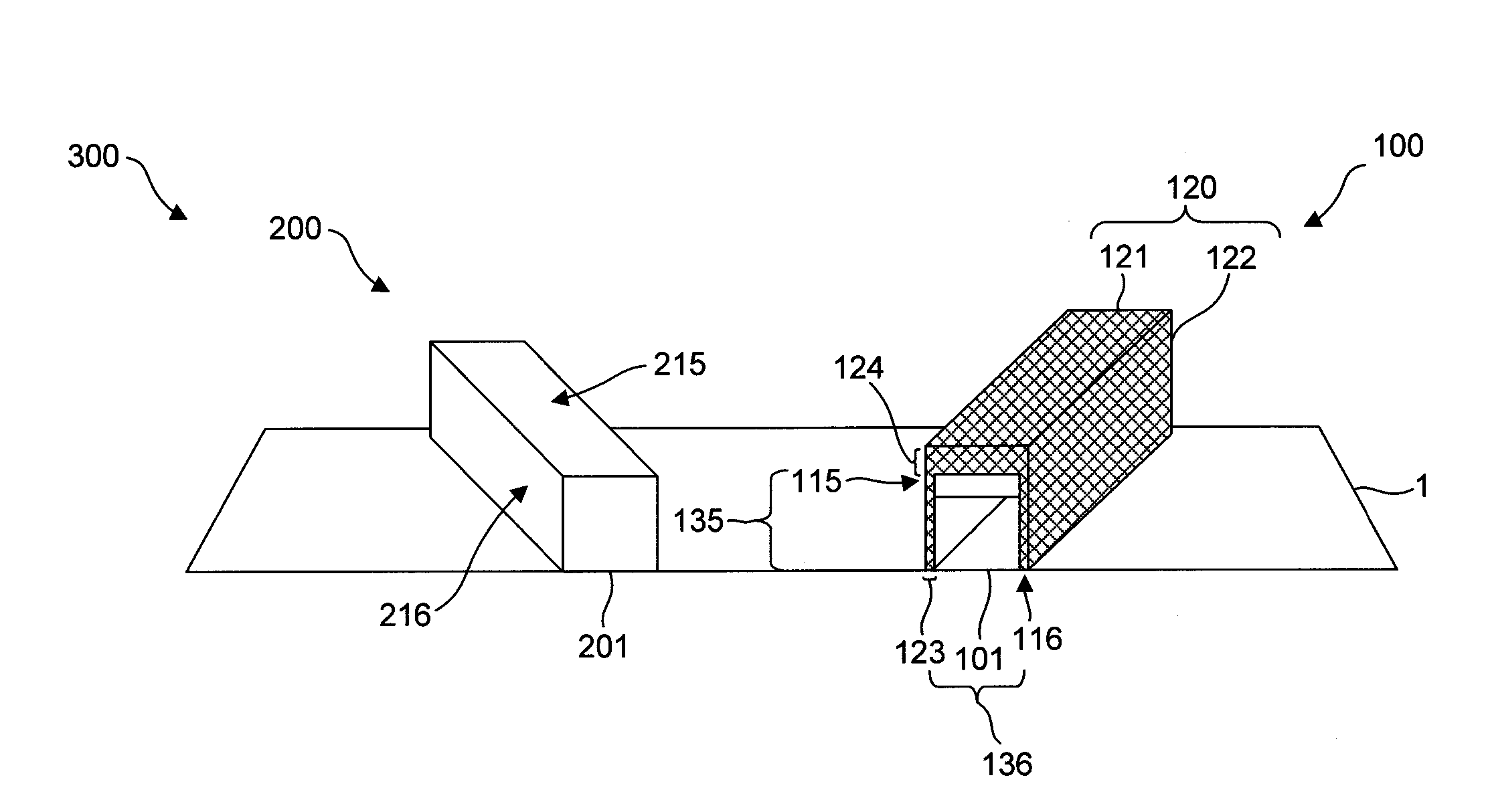
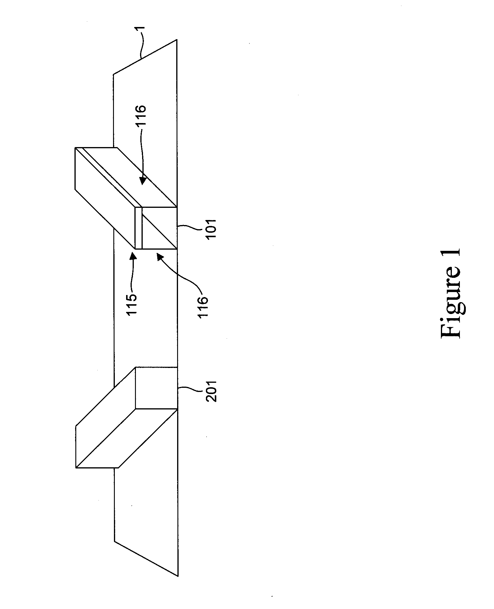
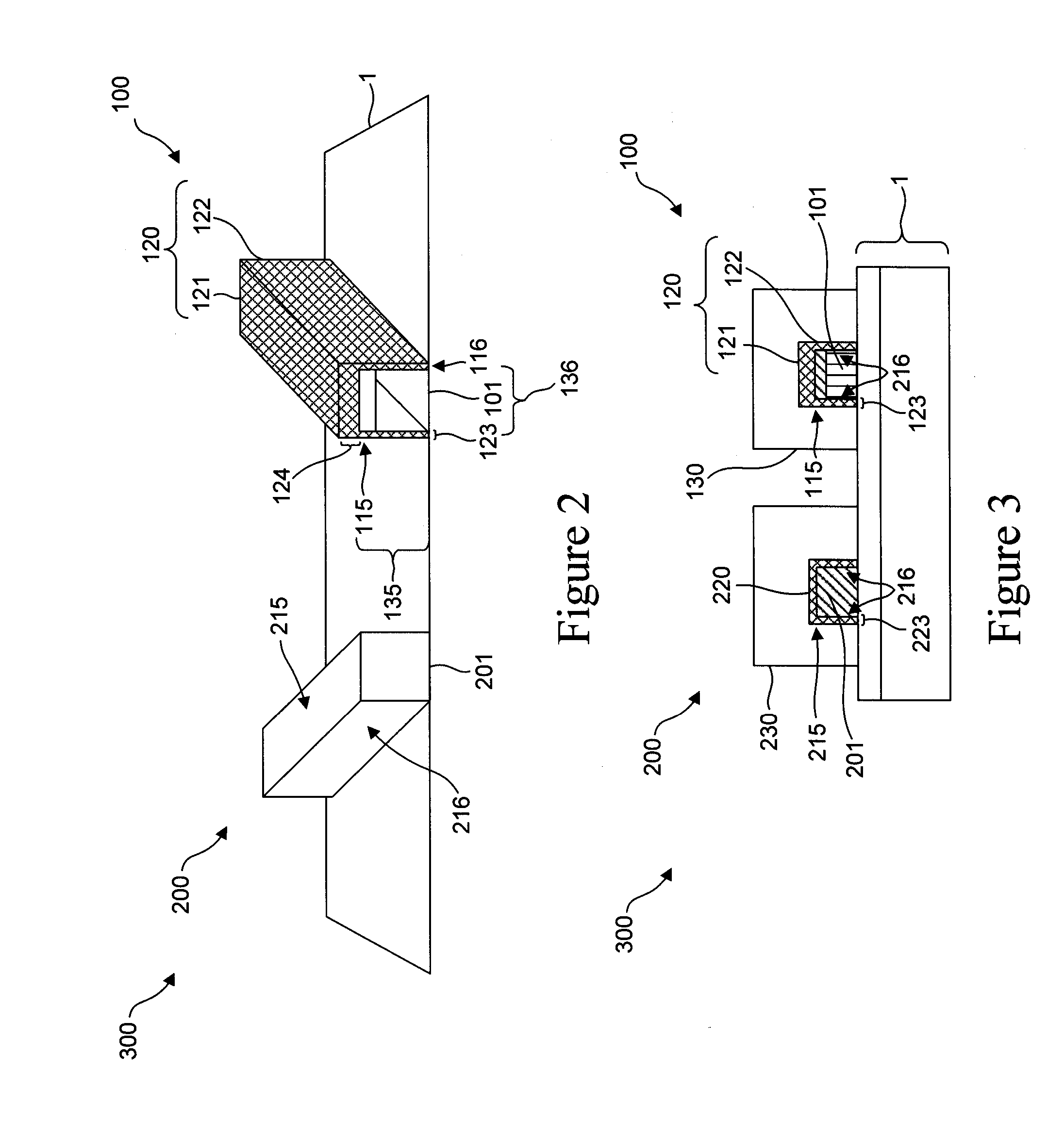
[0033] The present invention and the various features and advantageous details thereof are explained more fully with reference to the non-limiting embodiments that are illustrated in the accompanying drawings and detailed in the following description. It should be noted that the features illustrated in the drawings are not necessarily drawn to scale. Descriptions of well-known components and processing techniques are omitted so as to not unnecessarily obscure the present invention. The examples used herein are intended merely to facilitate an understanding of ways in which the invention may be practiced and to further enable those of skill in the art to practice the invention. Accordingly, the examples should not be construed as limiting the scope of the invention.

[0034] As discussed above, prior art methods of forming fins (i.e., semiconductor planes) having different crystalline orientations (e.g., {100}, {111}, {110}, {211}, {311}, {511} and {711}) ...


PUM


Abstract

Disclosed herein is a structure with two different type tri-gate MOSFETs formed on the same substrate. Each MOSFET comprises a fin with optimal mobility for the particular type of MOSFET. Due to the processes used to form fins with different crystalline orientations on the same substrate, one of the MOSFETs has a fin with a lower mobility top surface. To inhibit inversion of the top surface, this MOSFET has a gate dielectric layer with a thicker region on the top surface than it does on the opposing sidewall surfaces. Additionally, several techniques for forming the thicker region of the gate dielectric layer are also disclosed.

Description

BACKGROUND OF THE INVENTION [0001] 1. Field of the Invention [0002] The present invention relates generally to the field of semiconductor CMOS technology and, more particularly, to high mobility crystalline planes in tri-gate FinFET CMOS technology. [0003] 2. Description of the Related Art [0004] The mobility rates of holes and electrons through a p-channel and an n-channel of a p-type field effect transistor (p-FETs) and an n-type field effect transistor (n-FETs), respectively, effects delay. These mobility rates can be a function of the crystalline orientation of the semiconductor used to form the channel region. For example, delay can be minimized in a p-FET by forming the p-channel in a semiconductor having a 110 crystalline orientation which has the highest mobility for holes. Delay can be minimized in an n-FET by forming the channel in a semiconductor having a 100 crystalline orientation which has the highest mobility for electrons. Recent developments in FET technology allow ...

Claims


Application Information

Patent Timeline
IPC IPC(8): H01L29/76H01L21/336
CPCH01L21/823807H01L21/823821H01L21/823842H01L21/823857H01L29/785H01L27/1211H01L29/045H01L29/42384H01L21/845
Inventor ANDERSON, BRENT A.NOWAK, EDWARD J.
Owner ALSEPHINA INNOVATIONS INC
Why Eureka
Try Eureka