Structure and method for forming inter-poly dielectric in a shielded gate field effect transistor

a shielded gate field effect transistor and interpoly dielectric technology, which is applied in the direction of basic electric elements, electrical equipment, semiconductor devices, etc., can solve the problems of gate leakage, gate shortening, and inability to optimize the gate dielectric and the ipd independently

Active Publication Date: 2007-02-15
SEMICON COMPONENTS IND LLC
View PDF3 Cites 70 Cited by
  • Summary
  • Abstract
  • Description
  • Claims
  • Application Information

AI Technical Summary

Problems solved by technology

Second, conventional methods for forming the IPD typically introduce an oxide layer on the mesas between trenches that must be removed at some point after the gate electrode has been formed.
In removing this oxide some etching of the gate oxide down the trench sidewalls inevitably occurs, which may result in gate shorts and gate leakage.
This does not allow independent optimization of the gate dielectric and the IPD.

Method used


Image

  • Structure and method for forming inter-poly dielectric in a shielded gate field effect transistor
  • Structure and method for forming inter-poly dielectric in a shielded gate field effect transistor
  • Structure and method for forming inter-poly dielectric in a shielded gate field effect transistor

Examples


Embodiment Construction

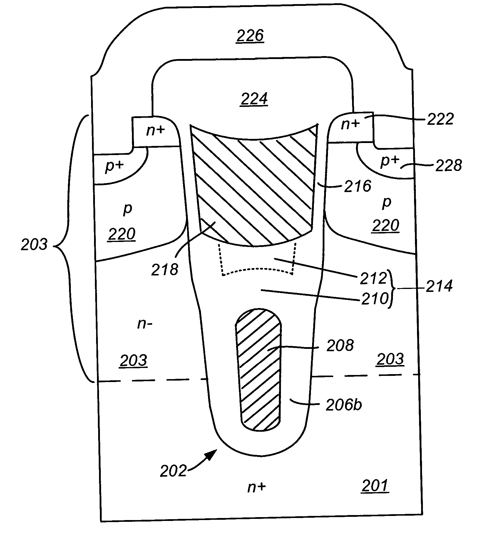
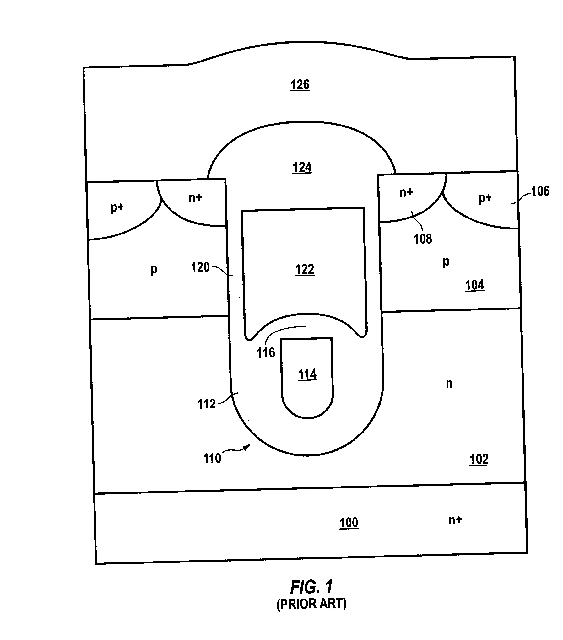
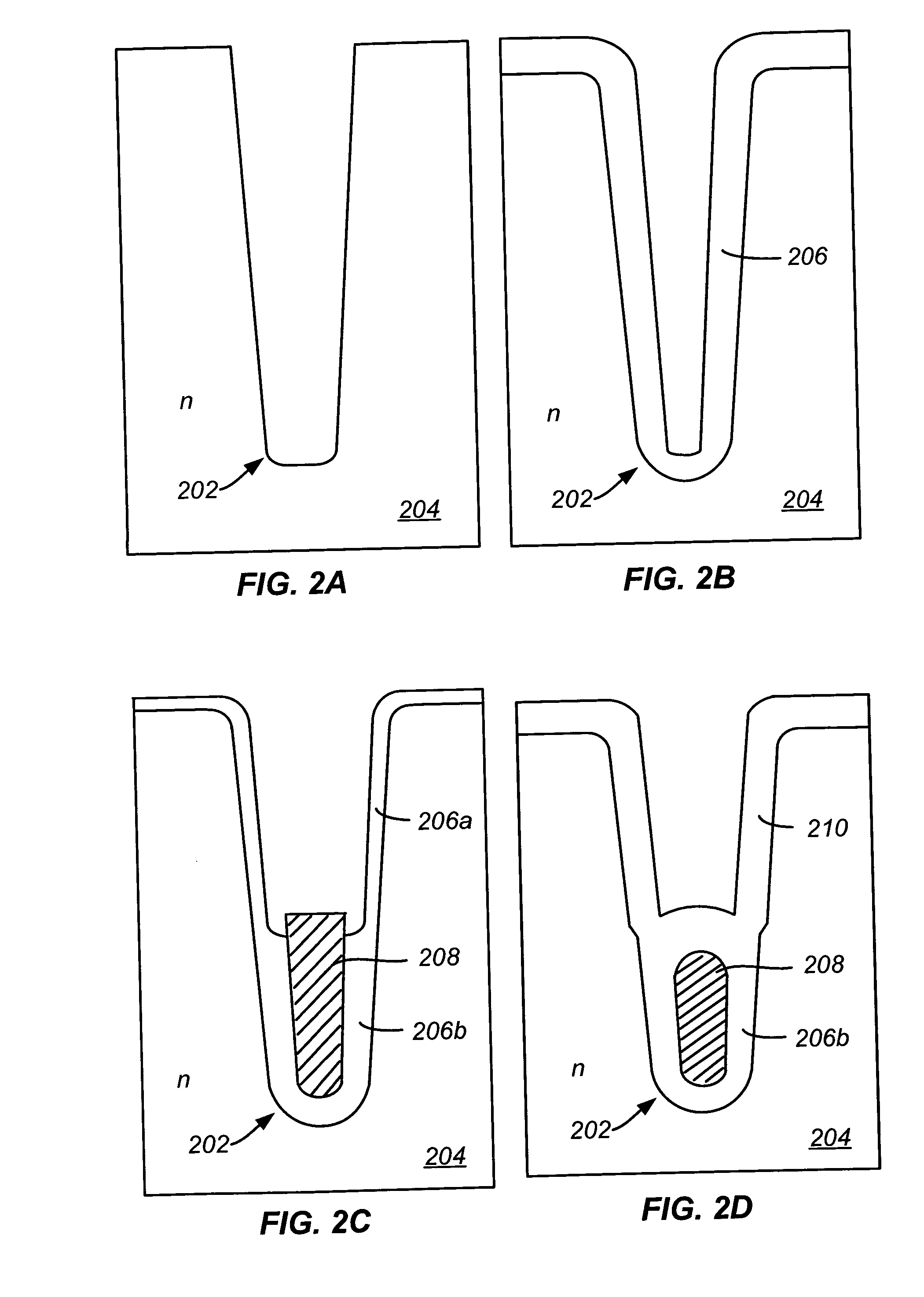
[0023] In accordance with the present invention, an IPD layer of a shielded gate FET is formed by performing a thermal oxidation followed by deposition of a conformal layer of dielectric. A gate dielectric is then formed, followed by formation of the gate electrode. This method decouples the process for forming the IPD layer from that for forming the gate dielectric, enabling each of these dielectric layers to be independently optimized. A high quality, thick IPD can thus be formed to support the required voltage between the gate and shield electrodes without compromising the gate dielectric quality or thickness. Further, the conformal layer of dielectric helps obtain a smooth concave profile (i.e., like the inside of a bowl) along the top surface of the IPD which in turn results in a smooth bottom profile for the gate electrode. This helps reduce the electric field as compared to the conventional FET structure in FIG. 1 where the gate electrode has sharp lower corners.

[0024]FIGS. ...


PUM


Abstract

A shielded gate trench FET is formed as follows. A trench is formed in a silicon region of a first conductivity type, the trench including a shield electrode insulated from the silicon region by a shield dielectric. An inter-poly dielectric (IPD) including a layer of thermal oxide and a layer of conformal dielectric is formed along an upper surface of the shield electrode. A gate dielectric lining at least upper trench sidewalls is formed. A gate electrode is formed in the trench such that the gate electrode is insulated from the shield electrode by the IPD.

Description

BACKGROUND OF THE INVENTION [0001] The invention relates in general to semiconductor power field effect transistors (FETs), and more particularly to a structure and method for forming an improved inter-poly dielectric (IPD) in a shielded gate FET. [0002] Shielded gate trench FETs are advantageous in that the shield electrode reduces the gate-drain capacitance (Cgd) and improves the breakdown voltage of the transistor. FIG. 1 is a simplified cross section view of a conventional shielded gate trench MOSFET. Trench 110 includes a shield electrode 114 directly below a gate electrode 122. Shield electrode 114 is insulated from adjacent silicon regions by a shield dielectric 112 which is generally thicker than gate dielectric 120. The gate and shield electrodes are insulated from one another by a dielectric layer 116 commonly referred to as inter-poly dielectric or IPD. The IPD layer must be of sufficient quality and thickness to support the required voltage between the gate and shield el...

Claims


Application Information

Patent Timeline
Patent Type & Authority Applications(United States)
IPC IPC(8): H01L21/84
CPCH01L29/407H01L29/4236H01L29/7813H01L29/66734H01L29/66727
Inventor HERRICK, ROBERTPROBST, DEANSESSION, FRED
Owner SEMICON COMPONENTS IND LLC
Why Eureka
Try Eureka