System and method for time resolved spectroscopy

a time-resolved spectroscopy and system technology, applied in the field of ccd devices, can solve the problems of not meeting the timing requirement of the laser scanning system, poor temporal resolution of the system, and much slower process, and achieve the effect of increasing the sampling speed and sensitivity

Inactive Publication Date: 2007-02-22
E2V TECH (UK) LTD
View PDF8 Cites 6 Cited by
  • Summary
  • Abstract
  • Description
  • Claims
  • Application Information

AI Technical Summary

Benefits of technology

[0008] We have appreciated the need for an improved detector arrangement for time resolved spectroscopy devices. In particular, we have appreciated the need for increased speed of sampling and sensitivity.

Problems solved by technology

In general these systems have poor temporal resolution.
This is a much slower process than the transfer into the store and would not meet the timing requirement of the laser scanning system.

Method used


Image

  • System and method for time resolved spectroscopy
  • System and method for time resolved spectroscopy
  • System and method for time resolved spectroscopy

Examples


first embodiment

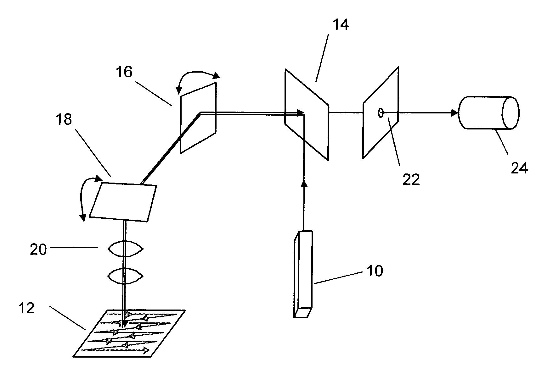
[0025] The basis of the first embodiment uses the “kinetic mode” concept. The mode of operation is as follows. As the scanning system scans across the sample, spectra are collected and stored within the storage region (e.g. 500 spectra). At the end of the line (i.e. when the laser reaches the boundary of the sample) the storage region is readout through the readout register and the multiplication register. The multiplication register provides almost noiseless gain within the charge domain thus allowing single photons to be detected. The readout of the store occurs as the laser returns to the beginning of the next line to be scanned.

[0026] If it is required that the whole target be sampled twice per second (500 spectra per line and 500 lines) and that half of the time is used to reposition the scanning laser from the end of a line to the beginning of the next, then this implies a time available to acquire one spectra is 1 microsecond. By the time the scan reaches the end of each line...

second embodiment

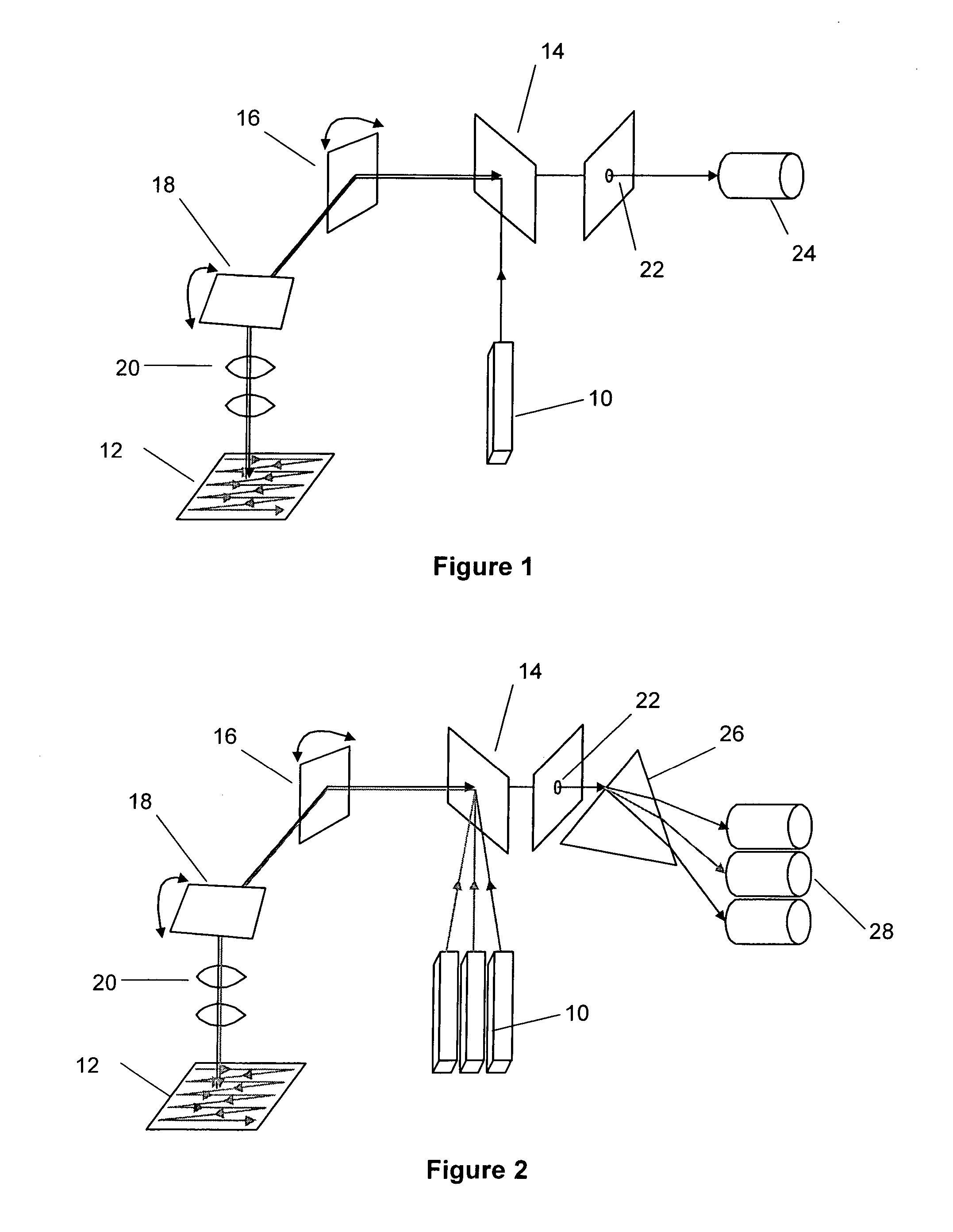
[0027] In order to minimise the data rate per output, multiple multiplication registers and outputs can be employed, as in the case illustrated in FIG. 5, which shows four multiplication registers and output amplifiers. In practice any number of registers can be employed. The output from the device may be simplified by the use of a multiplexer to recombine the outputs. With four multiplication registers, as shown, each multiplication register multiplies charge for a portion of the total photosites (and hence a portion of the total spectrum), in this case a quarter each. So, each multiplication register now only needs to be clocked at a quarter of the clocking speed of the arrangement of FIG. 4, namely 100 MHz÷4=25 MHz. This is a realistic and achievable speed with the result that the signal may be processed in the time available.

third embodiment

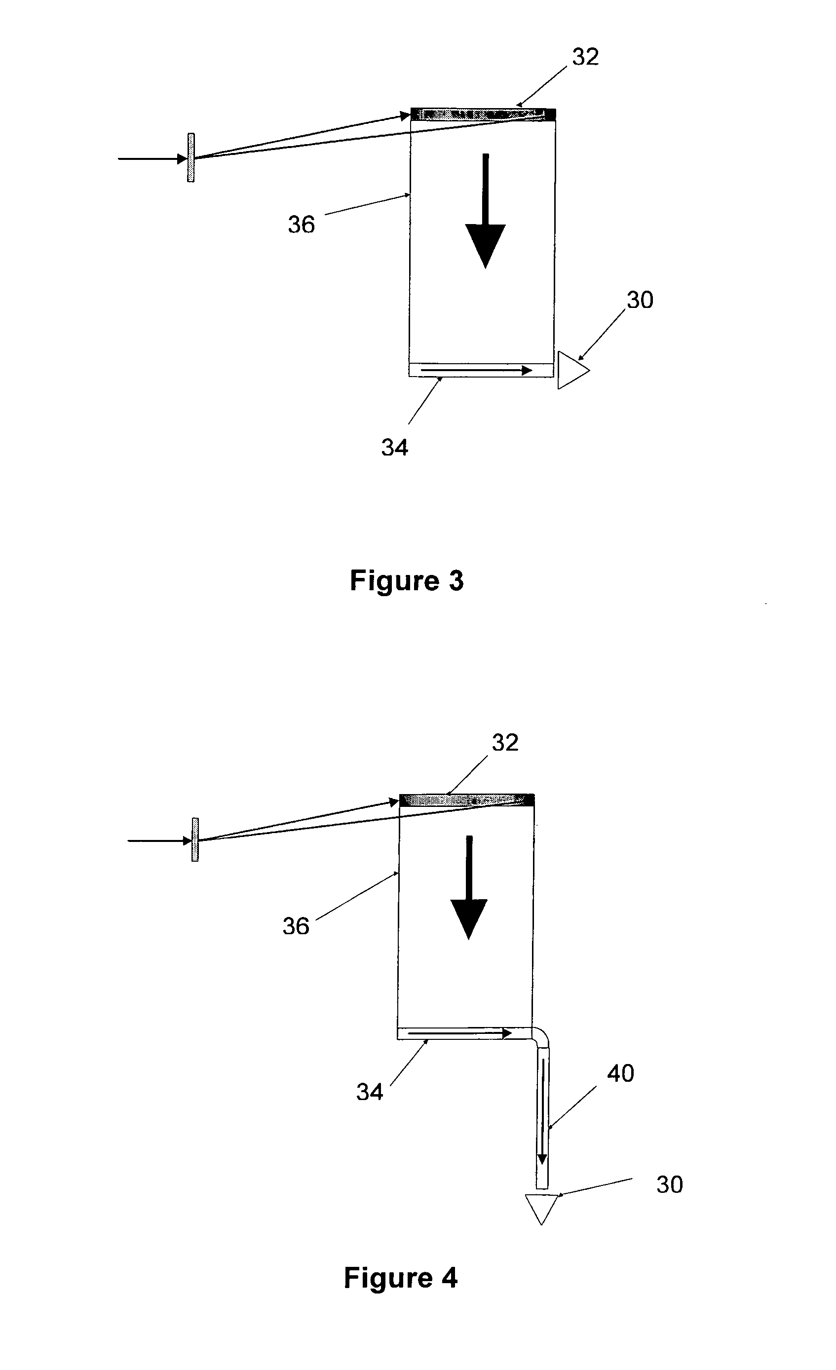
[0028] We have appreciated that the use of the store in FIG. 5 can be applied if there will be a time when spectra is not collected. For example, when the laser repositions from the end of one line to the beginning of the next. This time may not always be available. Therefore the following architecture and mode of operation is proposed in relation to a third embodiment shown in FIG. 6. The proposed device consists of an optically sensitive region 32 (made up of a small number of rows, typically one, and a number of columns, typically 96), an optically opaque region 36 into which the signal from the gathered spectra is transferred (this region may be omitted), a number of readout registers 34 and the same number of multiplication registers 40 and charge to voltage output amplifiers 30 (typically 8). A typical number of elements in each readout register is 12 and the typical number of elements in the multiplication register is 500-600. The multiplication registers are clocked at a pix...


PUM


Abstract

A system for time resolved spectroscopy comprises a CCD device arranged to receive a time varying spectrum. Time resolved spectroscopy is the analysis of a spectrum that varies with time due to any cause. The variation with time of the spectrum may be due, for example, to (i) changes of the spectrum from a given sample space with time (such as due to emission decay); and (ii) changes in the spectrum as successive portions of a sample space are sampled (such as laser scanning microscopy). The CCD device comprises an array of photosites arranged to detect the time varying spectrum and to produce signal charge representative of the spectrum, and one or more CCD multiplication registers arranged to receive the signal charge and to provide charge multiplication. An enhancement of speed and sensitivity is given by a storage area which receives the signal charge in parallel from the array of photosites to provide the charge in serial to the one or more multiplication registers.

Description

CROSS-REFERENCE TO RELATED APPLICATIONS [0001] This application claims priority from Application No. GB 0516989.1 filed Aug. 18, 2005 in the United Kingdom. FIELD OF THE INVENTION [0002] The present invention relates to CCD devices, in particular to CCD devices for use in time resolved spectroscopy devices. BACKGROUND OF THE INVENTION [0003] The concept behind fluorescence microscopy is as follows. Fluorescent dye molecules can be attached to specific parts of the biological sample of interest. When excited by a suitable wavelength of light these markers fluoresce so that only those parts are seen in the microscope. More than one type of fluorescent dye can be used in the sample to attach to different features. By changing the wavelength of the excitation light, different types of dye can be forced to fluoresce thus enabling different structures within the sample to be distinguished. The dyes can be chosen to fluoresce at different wavelengths. Thus if the sample is excited by a spe...

Claims


Application Information

Patent Timeline
Patent Type & Authority Applications(United States)
IPC IPC(8): G01J3/45H01L27/148H01L29/768
CPCH01L27/14806H01L29/76816
Inventor ROBBINS, MARK STANFORDBELL, RAYMOND THOMAS
Owner E2V TECH (UK) LTD
Why Eureka
Try Eureka