Semiconductor storage device

Active Publication Date: 2007-02-22
XENOGENIC DEV LLC
View PDF5 Cites 55 Cited by
  • Summary
  • Abstract
  • Description
  • Claims
  • Application Information

AI Technical Summary

Benefits of technology

[0042] According to the semiconductor storage device of the ninth feature, the number of the memory cells in each column can be increased without increasing the total number of the memory cells connected to the bit lines, hence minimizing the current to be driven by the bit line selecting transistors and increasi

Problems solved by technology

This may hardly permit the current Ids to run through the selected data line.
As the result, the conventional ½ bias mode fails to supply the selected data line with a proper level of the current, hence disabling the writing action with desired writing characteristics.
As the result, the conventional ⅓ bias mode fails to supply the selected data line with a proper level of the current particularly when the transistor width of the data line selecting transistors i

Method used


Image

  • Semiconductor storage device
  • Semiconductor storage device
  • Semiconductor storage device

Examples


first embodiment

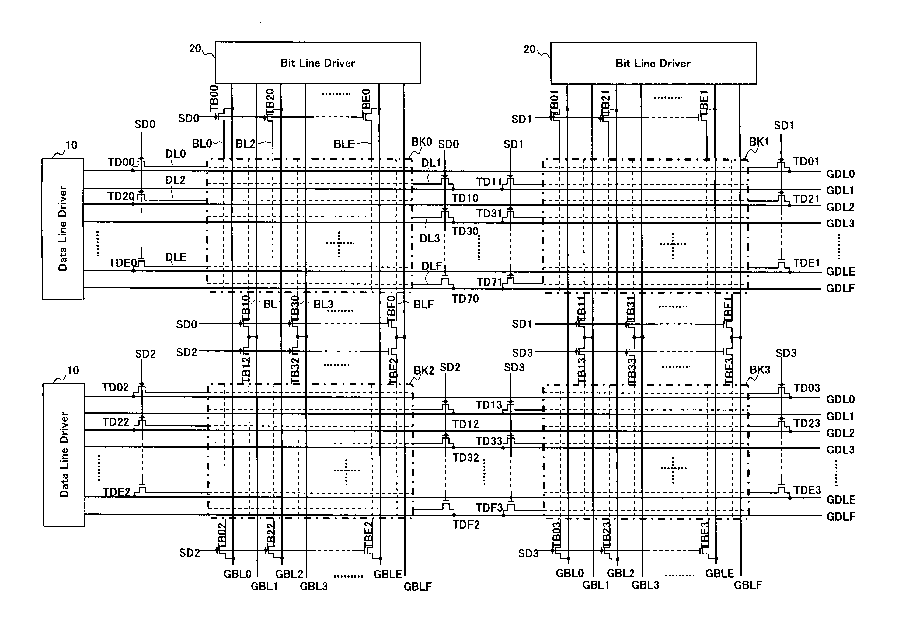
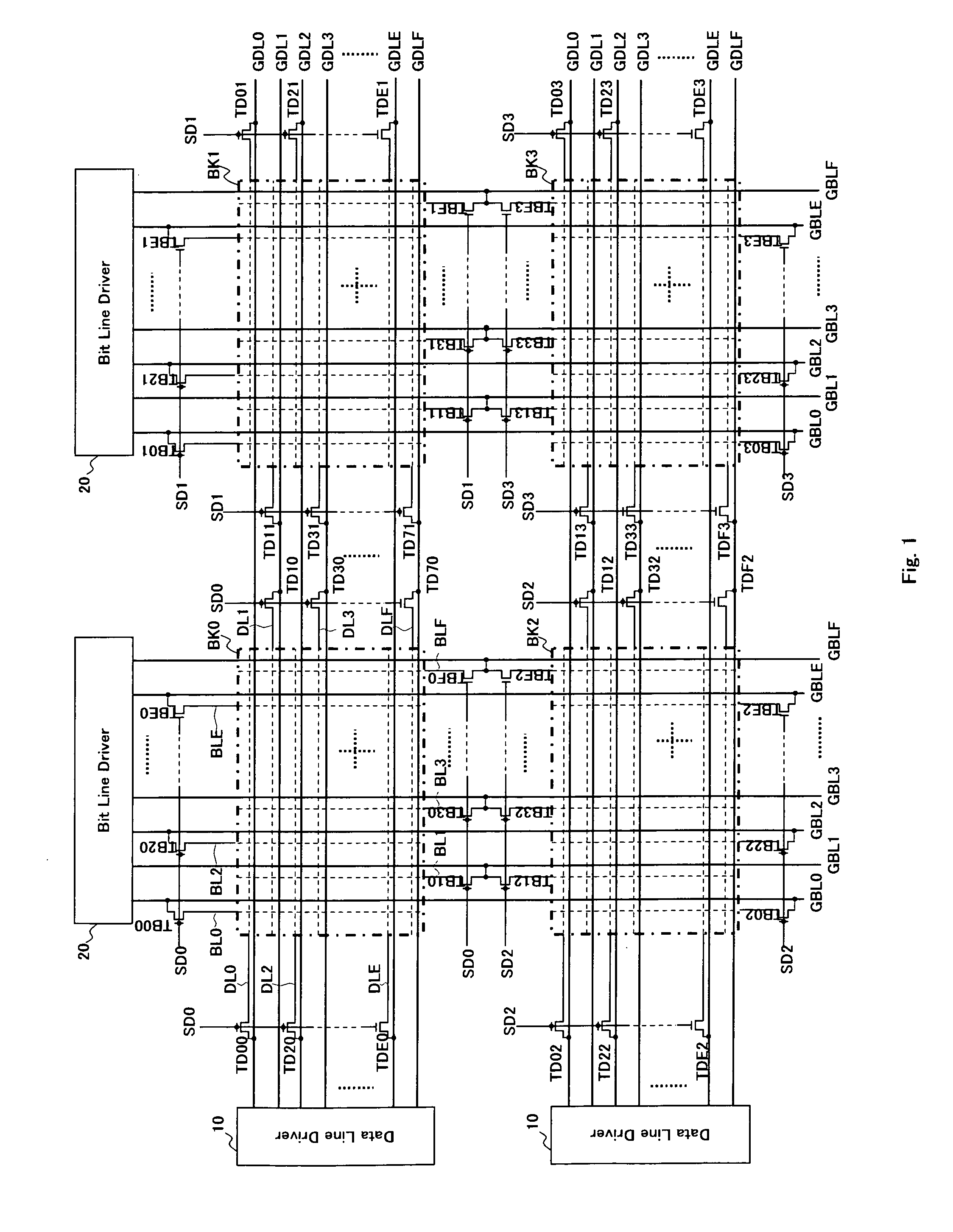
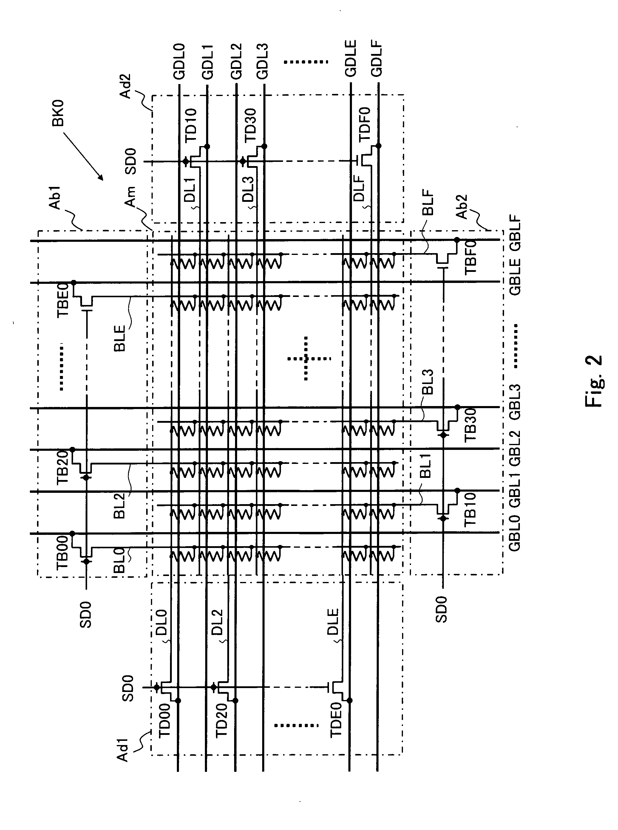
[0061]FIG. 1 is a block diagram of an array of memory cells of the inventive device in the form of a cross point memory of a multi-bank type. As shown in FIG. 2, each of banks BKk (k ranging from 0 to 3) comprises a memory cell array of the cross point type where the memory cells, each including a variable resistor element of which the electrical resistance is varied to save a data, are arranged in a matrix of rows by columns with a number of data lines DLi extending along the rows and a number of bit lines BLj extending along the columns. A group of the memory cells along each row are connected at one end of their variable resistor elements to a common data line while another group of the memory cells along each column are connected at the other end of their variable resistor elements to a common bit line. The data lines DLi and the bit lines BLj of each bank BKk shown in FIG. 1 are briefly denoted by the broken lines while the memory cells are not illustrated for simplicity. The b...

second embodiment

[0096] A second embodiment of the present invention will be described. The inventive device of the second embodiment is also a cross point memory of the multi-bank type similar to that of the first embodiment. As the block arrangement is identical to that of the first embodiment shown in FIGS. 1 and 2, its overlapping description will be omitted. The second embodiment is differentiated from the first embodiment by an action of the bias mode for supplying each of the data lines DLi and each of the bit lines BLj in a target bank (for example, the bank BK0) with a row potential and a column potential respectively to conduct the writing action. The bias mode will now be described in more detail. It is assumed in the second embodiment similar to the first embodiment that the data line selecting transistors TDik are lower in the current driving capability than the bit line selecting transistors TBjk and one of the memory cells in a 16×16 array is a target memory cell to be written.

[0097]...

third embodiment

[0113] A third embodiment of the present invention will be described. The inventive device of the third embodiment is also a cross point memory of the multi-bank type similar to that of the first or second embodiment. As the block arrangement is identical to that of the first embodiment shown in FIGS. 1 and 2, its overlapping description will be omitted. The third embodiment is differentiated from the first embodiment by an action of the bias mode for supplying each of the data lines DLi and each of the bit lines BLj in a target bank (for example, the bank BK0) with a row potential and a column potential respectively to conduct the writing action. The bias mode will now be described in more detail. It is assumed in the third embodiment similar to the first or second embodiment that the data line selecting transistors TDik are lower in the current driving capability than the bit line selecting transistors TBjk and one of the memory cells in a 16×16 array is a target memory cell to be...


PUM


Abstract

In a semiconductor storage device with cross point type arrays of memory cells including variable resistor elements, a selected data line and unselected data lines are supplied with a row selecting potential and a row unselecting potential through a data line selecting transistor respectively, a selected bit line and unselected bit lines are supplied with a column selecting potential and a column unselecting potential through a bit line selecting transistor respectively. Data lines and bit lines are separately driven so that when the data line selecting transistor is higher in the current driving capability than the bit line selecting transistor, a second bias voltage between the row unselecting potential and column selecting potential is lower than a first bias voltage between the row selecting potential and column unselecting potential, in the opposite case, the first bias voltage is lower than the second voltage.

Description

CROSS REFERENCE TO RELATED APPLICATION [0001] This Nonprovisional application claims priority under 35 U.S.C. §119(a) on Patent Application No. 2005-236285 filed in Japan on Aug. 17, 2005, the entire contents of which are hereby incorporated by reference. BACKGROUND OF THE INVENTION [0002] 1. Field of the Invention [0003] The present invention relates to a semiconductor storage device which comprises an array of memory cells, each memory cell consisting mainly of a variable resistor element of which the electric resistance is varied to save a data, arranged in rows and columns at a cross point mode where each row of the memory cells are connected at one end to a common data line and each column of the memory cells are connected at the other end to a common bit line. Particularly, the present invention relates to a semiconductor storage device which comprises a memory cell array of a cross point type where each variable resistor element is varied in the resistance by application of e...

Claims


Application Information

Patent Timeline
IPC IPC(8): G11C11/00
CPCG11C7/12G11C7/18G11C8/08G11C13/0004G11C13/0007G11C13/0026G11C13/0028G11C13/0069G11C2013/009G11C2213/31G11C2213/32G11C2213/34G11C2213/77
Inventor INOUE, KOHJI
Owner XENOGENIC DEV LLC
Why Eureka
Try Eureka