Silicon carbide semiconductor device having high channel mobility and method for manufacturing the same

a silicon carbide semiconductor and high-channel technology, applied in semiconductor/solid-state device manufacturing, semiconductor devices, electrical devices, etc., can solve the problem of insufficient channel mobility, and achieve the effect of high-channel mobility

Active Publication Date: 2007-03-01
DENSO CORP
View PDF14 Cites 83 Cited by
  • Summary
  • Abstract
  • Description
  • Claims
  • Application Information

AI Technical Summary

Benefits of technology

[0007] The above device is characterized in that dangling bond of an interface of the channel area and the gate insulating film is terminated by an element of H or OH, and hydrogen concentration at the interface is set to 2.6×1020 cm−3 or more. Thus, if the dangling bond of the interface of the channel area and the gate insulating film is terminated by the element of H or OH, and the hydrogen concentration at the interface is set to a high value of 2.6×1020 cm−3 or more, it is possible to set a silicon carbide semiconductor device of high channel mobility.

Problems solved by technology

However, it is not still sufficient in the channel mobility obtained in a technique shown in U.S. Pat. No. 6,764,963, and it is expected to intend a further improvement of the channel mobility.

Method used


Image

  • Silicon carbide semiconductor device having high channel mobility and method for manufacturing the same
  • Silicon carbide semiconductor device having high channel mobility and method for manufacturing the same
  • Silicon carbide semiconductor device having high channel mobility and method for manufacturing the same

Examples


first embodiment

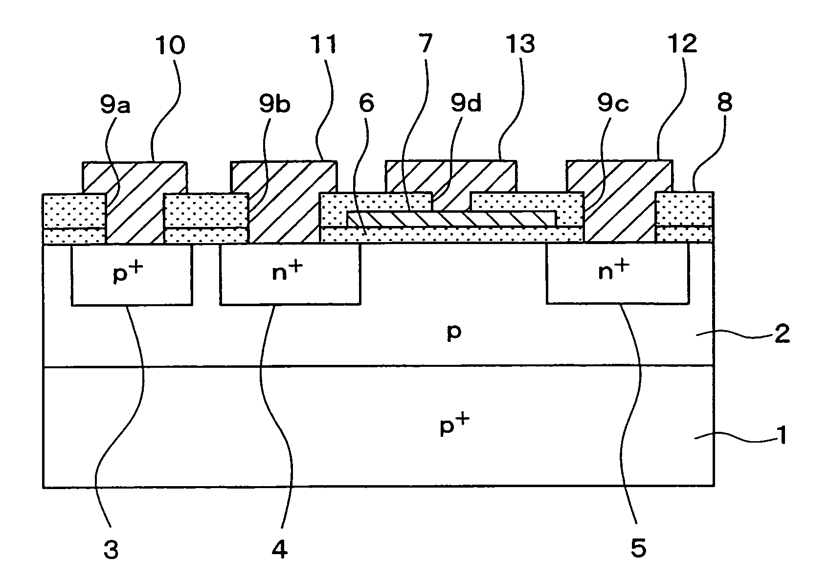
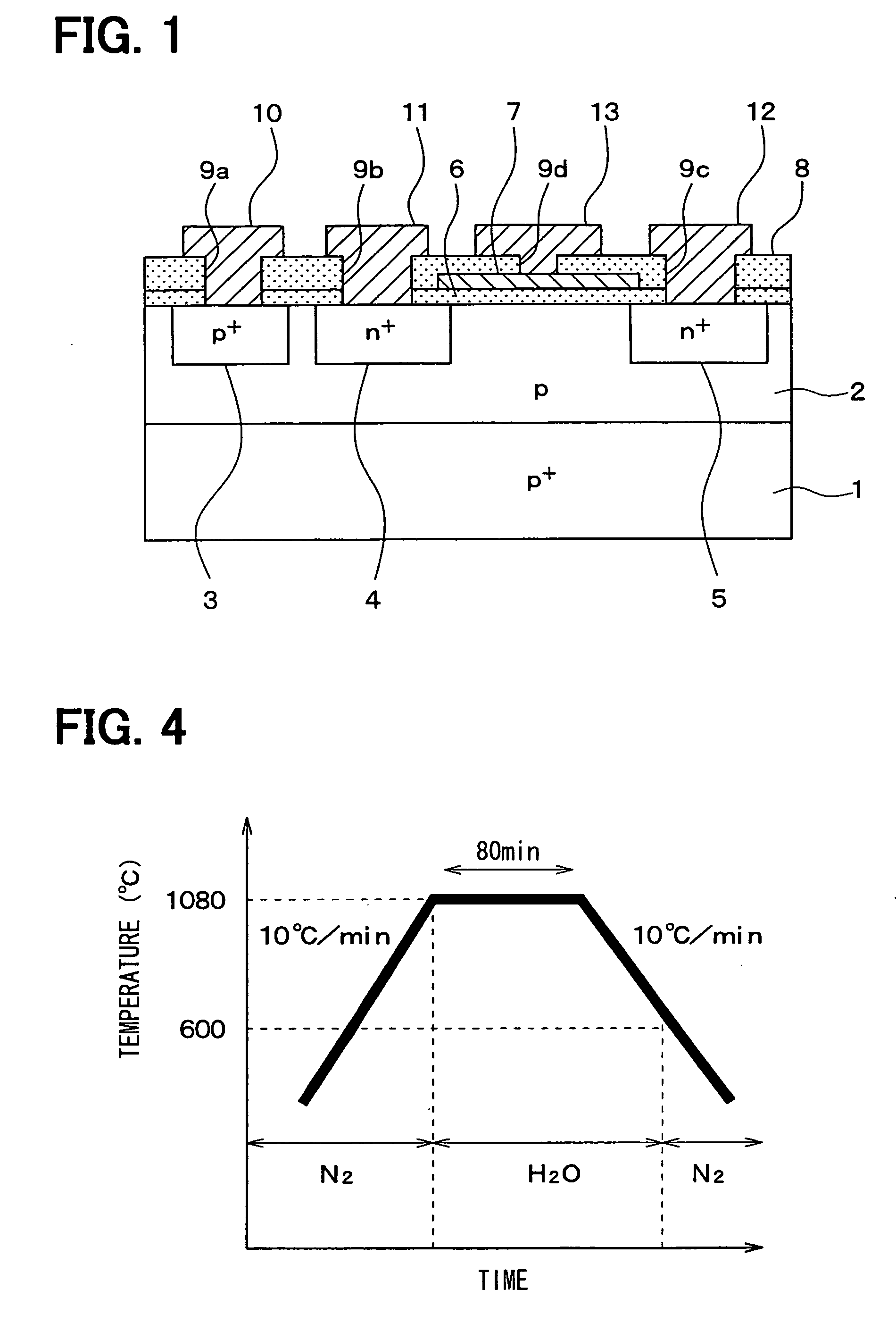
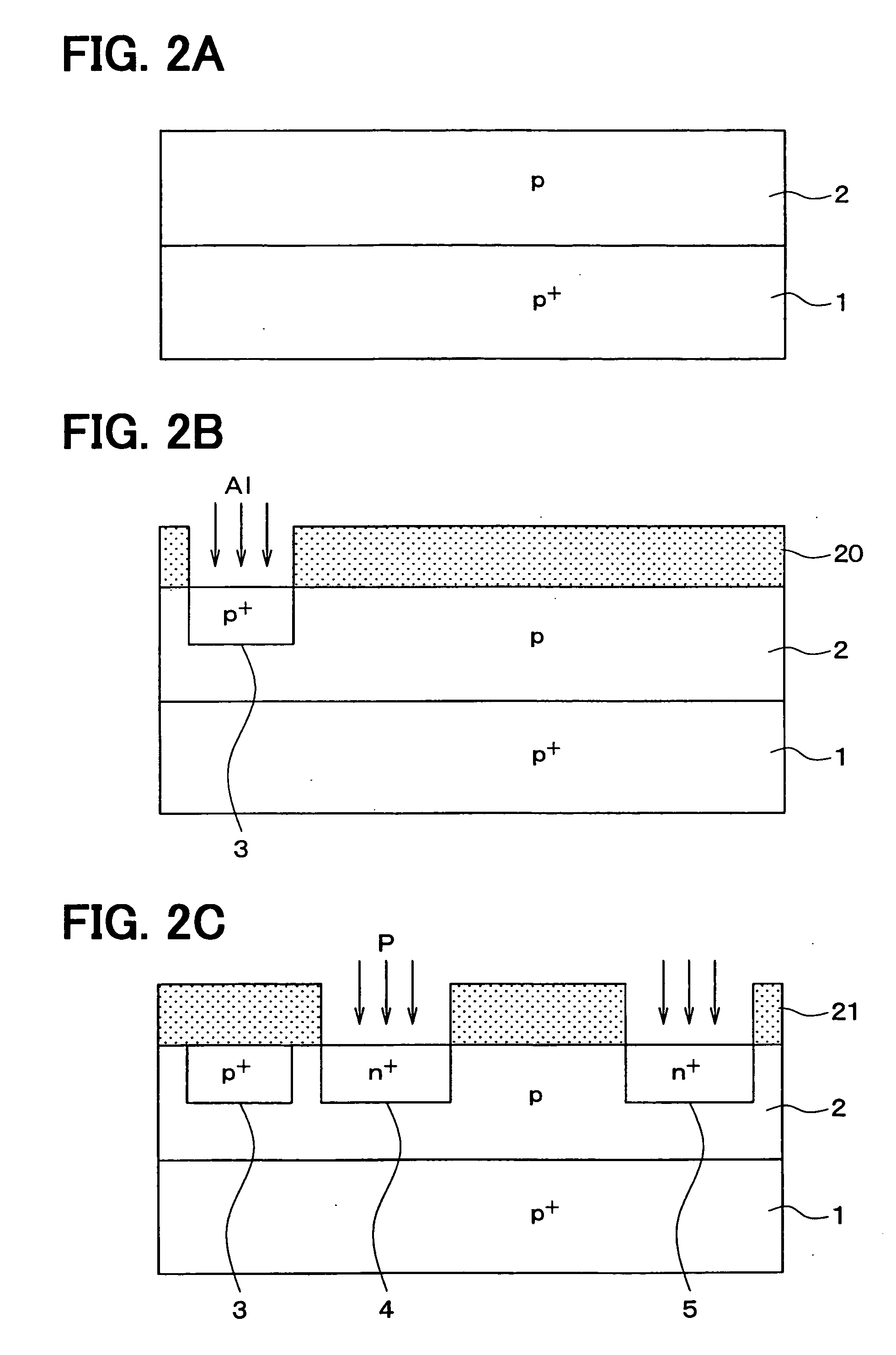
[0105] A first embodiment mode of the present invention will be explained. In this embodiment mode, one embodiment mode of the present invention is applied to an inversion type lateral MOSFET. FIG. 1 shows a sectional construction of the inversion type lateral MOSFET. FIGS. 2 and 3 show manufacturing processes of the inversion type lateral MOSFET shown in FIG. 1. The structure of the inversion type lateral MOSFET of this embodiment mode and its manufacturing method will be explained with reference to these figures.

[0106] As shown in FIG. 1, one face side of a substrate 1 of a p+ type constructed by SiC is set to a main surface, and a p / p+ substrate forming a p type base layer 2 constructed by SiC epitaxially grown on the main surface is used as a semiconductor substrate. For example, the substrate 1 of the p+ type is constructed by 4H—SiC and the main surface is set to face a, i.e., a (11-20)-plane and impurity concentration is set to about 533 1018 cm−3. For example, the impurity ...

second embodiment

Mode

[0126] A second embodiment mode of the present invention will be explained. In this embodiment mode, one embodiment mode of the present invention is also applied to the inversion type lateral MOSFET. However, this embodiment mode differs from the first embodiment mode in that the manufacturing method of the inversion type lateral MOSFET is partially changed. The structure of the inversion type lateral MOSFET, etc. in this embodiment mode are similar to those in the first embodiment mode. The inversion type lateral MOSFET of this embodiment mode will next be explained. However, the explanation will be made with respect to only different points from the first embodiment mode, and is omitted with respect to portions similar to those of the first embodiment mode.

[0127] The inversion type lateral MOSFET of this embodiment mode is manufactured by adding a manufacturing process shown in FIG. 6 to the manufacturing method of the inversion type lateral MOSFET shown in FIGS. 2 and 3 in t...

third embodiment

Mode

[0135] A third embodiment mode of the present invention will be explained. In this embodiment mode, one embodiment mode of the present invention is also applied to the inversion type lateral MOSFET. However, this embodiment mode differs from the first or second embodiment mode in that the manufacturing method of the inversion type lateral MOSFET is partially changed. The structure of the inversion type lateral MOSFET, etc. in this embodiment mode are similar to those in the first or second embodiment mode. The inversion type lateral MOSFET of this embodiment mode will next be explained. However, only different points from the first or second embodiment mode will be explained, and the explanations of portions similar to those of the first or second embodiment mode are omitted.

[0136] The inversion type lateral MOSFET of this embodiment mode is manufactured by changing the forming process of the interlayer insulating film 8 shown in FIG. 3C to processes shown in FIGS. 8A and 8B am...


PUM


Abstract

A silicon carbide semiconductor device having a MOS structure includes: a substrate; a channel area in the substrate; a first impurity area; a second impurity area; a gate insulating film on the channel area; and a gate on the gate insulating film. The channel area provides an electric current path. The channel area and the gate insulating film have an interface therebetween. The interface includes a dangling bond, which is terminated by a hydrogen atom or a hydroxyl. The interface has a hydrogen concentration equal to or larger than 2.6×1020 cm−3.

Description

CROSS REFERENCE TO RELATED APPLICATIONS [0001] This application is based on Japanese Patent Applications No. 2005-251365 filed on Aug. 31, 2005, and No. 2006-162448 filed on Jun. 12, 2006, the disclosures of which are incorporated herein by reference. FIELD OF THE INVENTION [0002] The present invention relates to a silicon carbide semiconductor device having high channel mobility and a method for manufacturing the same. BACKGROUND OF THE INVENTION [0003] It is conventionally disclosed in U.S. Pat. No. 6,764,963 that the channel mobility in the MOS structure can be improved by performing processing in hydrogen anneal or a wet atmosphere in the SiC semiconductor device in which face a set to a (11-20)-plane in the plane azimuth of a crystal face is used in a channel. Concretely, it is intended that the channel mobility is improved by selecting concentration or temperature of the hydrogen anneal or the wet atmosphere. [0004] However, it is not still sufficient in the channel mobility o...

Claims


Application Information

Patent Timeline
Patent Type & Authority Applications(United States)
IPC IPC(8): H01L31/0312
CPCH01L21/049H01L29/045H01L29/0847H01L29/513H01L29/7838H01L29/66068H01L29/78H01L29/7828H01L29/518
Inventor ENDO, TAKESHIYAMAMOTO, TSUYOSHIKAWAI, JUNYAMAMOTO, KENSAKUOKUNO, EIICHI
Owner DENSO CORP
Why Eureka
Try Eureka