Organic light emitting display and method for fabricating the same

a technology of light-emitting display and organic material, which is applied in the direction of discharge tube luminescnet display, discharge tube/lamp details, electric discharge lamps, etc., can solve the problems of high cost of laser equipment, difficulty in improving the quality of a transfer layer, and difficulty in making displays with improved life span, so as to improve the life span and improve the effect of low luminous efficiency

Inactive Publication Date: 2007-03-01
SAMSUNG DISPLAY CO LTD
View PDF5 Cites 96 Cited by
  • Summary
  • Abstract
  • Description
  • Claims
  • Application Information

AI Technical Summary

Benefits of technology

[0011] Accordingly, it is an object of the present invention to provide an organic light emitting display and a method for fabricating the same, wherein a layout of respective pixels is changed in order to improve life span so that one pixel region having low luminous efficiency is increased.
[0012] It is another object of the present invention to provide an organic light emitting display and a method for fabricating the same, wherein the number of masks for forming an emission layer is reduced.

Problems solved by technology

Specifically, since there are limits to the fabrication of a sub pixel region of a certain color, it is difficult to make displays having improved life span.
In response to this problem, a laser thermal transfer method has been proposed, but this method is characterized by the disadvantages of the high cost of laser equipment, and the difficulty of improving the quality of a transfer layer.
However, in this case, there is a problem of misalignment, and the resolution of the display deteriorates as a result.
In addition, manufacturing cost increases and a more precise patterning technique is required.

Method used


Image

  • Organic light emitting display and method for fabricating the same
  • Organic light emitting display and method for fabricating the same
  • Organic light emitting display and method for fabricating the same

Examples


first embodiment

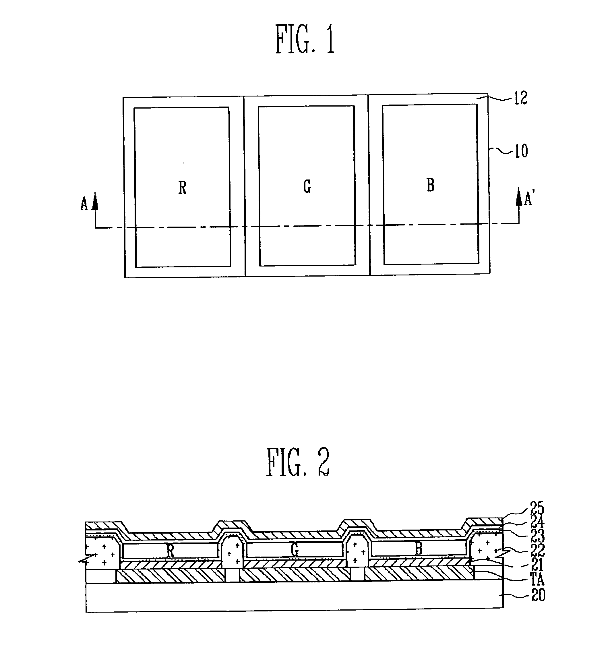
[0057]FIG. 4 is a plan view of one pixel region shown in FIG. 3 as a layout of the organic light emitting display according to the present invention.

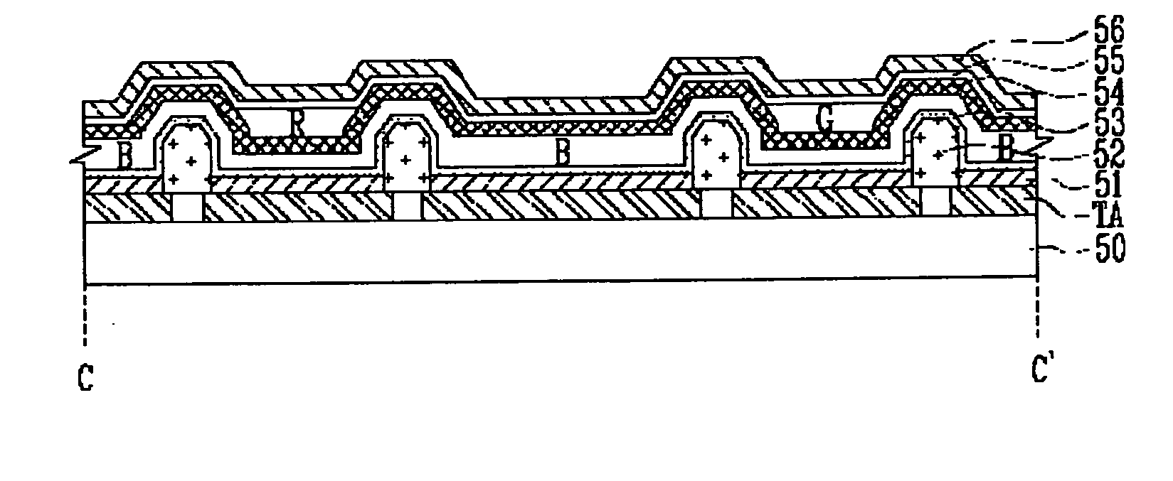
[0058] Referring to FIG. 4, one pixel region 40 includes red (R), green (G) and blue (B) sub pixel regions. The red (R), green (G) and blue (B) sub pixel regions have areas different from each other. In particular, the blue (B) sub pixel region having relatively lower luminous efficiency is formed over an entire surface of the pixel region 40 in common. The red (R) and green (G) sub pixel regions are formed at a closed curve of the blue (B) sub pixel region so as not to overlap each other. In detail, the red (R) and green (G) sub pixel regions are formed in a stripe pattern with the blue (B) sub pixel region disposed therebetween. Furthermore, the blue (B) sub pixel region is always disposed at a peripheral portion of the pixel region 40.

[0059] A forming area of the blue (B) sub pixel, except forming areas of the red (R) and s green (G...

second embodiment

[0108]FIG. 11 is a plan view of the one pixel region shown in FIG. 3 as a layout of the organic light emitting display according to the present invention.

[0109] Referring to FIG. 11, one pixel region 110 includes red (R), green (G), and blue (B) sub pixel regions. The red (R), green (G) and blue (B) sub pixel regions have different areas from each other. In particular, the blue (B) sub pixel region having relatively lower luminous efficiency is formed over an entire surface of the pixel region 110 in common. The red (R) and green (G) sub pixel regions are formed in a blue (B) closed curve so as not to overlap each other. The red (R) sub pixel region is formed at an upper left portion of the pixel region 110, whereas the green (G) sub pixel region is formed at a lower right portion of the pixel region 110. The red (R), green (G) and blue (B) sub pixels are arranged in a delta pattern having a triangular shape. Each of the red (R), green (G) and blue (B) sub pixel regions has a square...

third embodiment

[0111]FIG. 12 is a plan view of one pixel region shown in FIG. 3 as a layout of the organic light emitting display according to the present invention.

[0112] Referring to FIG. 12, one pixel region 120 includes red (R), green (G) and blue (B) sub pixel regions. The red (R), green (G) and blue (B) sub pixel regions have different areas from each other. In particular, the blue (B) sub pixel region having relatively lower luminous efficiency is formed over an entire surface of the pixel region 120 in common. The red (R) and green (G) sub pixel regions are formed in a blue (B) closed curve so as not to overlap each other. The red (R) sub pixel region is formed at an upper left portion of the pixel region 120, whereas the green (G) sub pixel region is formed at an upper right portion of the pixel region 120. The red (R), green (G) and blue (B) sub pixels are arranged in a delta pattern having a triangular shape. Although the pixel region 120 of FIG. 12 has a construction similar to that of...


PUM


Abstract

In an organic light emitting display and a method for fabricating the same, a layout of respective pixels is changed in order to improve life span so that one pixel region having low luminous efficiency is increased. The organic light emitting display includes at least one pixel comprising sub pixels having a plurality of colors. A first sub pixel emission layer is formed over an entire surface of a pixel region. At least two second sub pixel emission layers are formed at the first sub pixel emission layer so as to have a closed curve. The layout of respective pixels is changed so as to increase an area of one sub pixel region having low luminous efficiency in order to improve the life span and aperture ratio of the organic light emitting display. In addition, during formation of an emission layer, the number of masks is reduced. Accordingly, the possibility of misalignment is reduced, thereby maximizing resolution, improving yield, and reducing manufacturing cost.

Description

CLAIM OF PRIORITY [0001] This application makes reference to, incorporate the same herein, and claims all benefits accruing under 35 U.S.C. § 119 from an application for ORGANIC LIGHT EMITTING DISPLAY AND METHOD FOR FABRICATING THE SAME earlier filed in the Korean Intellectual Property Office on 26 Aug. 2005 and there duly assigned Serial No. 10-2005-0079063. BACKGROUND OF THE INVENTION [0002] 1. Technical Field [0003] The present invention relates to an organic light emitting display and a method for fabricating the same. More particularly, the present invention relates to an organic light emitting display and a method for fabricating the same, wherein a layout of respective pixels is changed in order to improve life duration so that one pixel region having low luminous efficiency is increased. [0004] 2. Related Art [0005] Recently, various flat plate displays capable of reducing weight and volume, which are disadvantages of cathode ray tubes (CRT), have been developed. Flat panel ...

Claims


Application Information

Patent Timeline
Patent Type & Authority Applications(United States)
IPC IPC(8): H01L51/00
CPCH01L51/56H01L27/3218H01L27/3216H10K59/352H10K59/353H10K71/00H05B33/14H05B33/10
Inventor KIM, BYUNG HEE
Owner SAMSUNG DISPLAY CO LTD
Why Eureka
Try Eureka