

Delay adjustment circuit and synchronous semiconductor device having the delay adjustment circuit
- Summary
- Abstract
- Description
- Claims
- Application Information
AI Technical Summary
Benefits of technology
Problems solved by technology
Method used
Image

Examples
Embodiment Construction
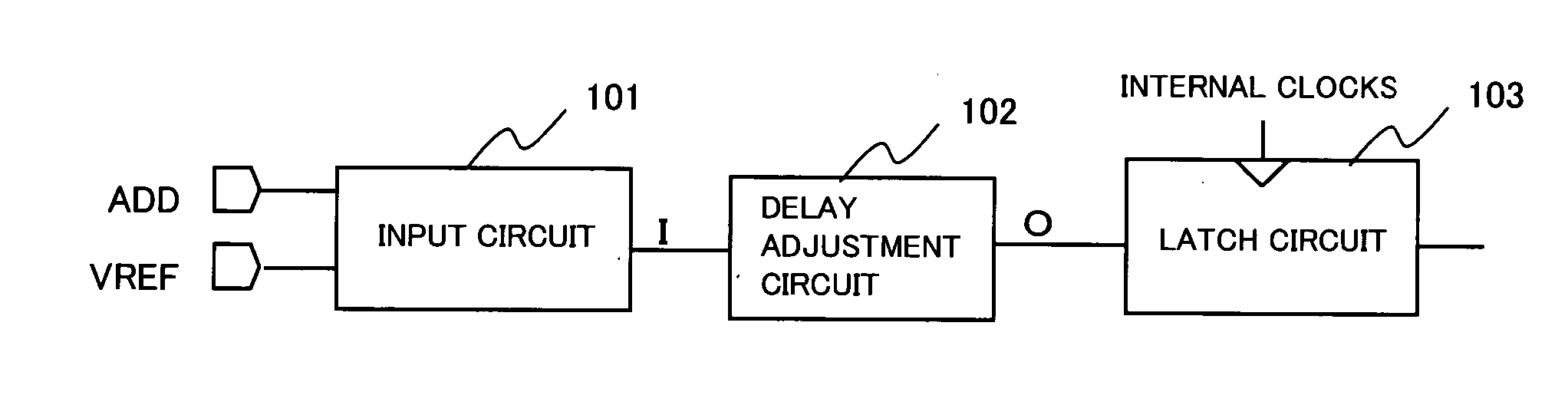
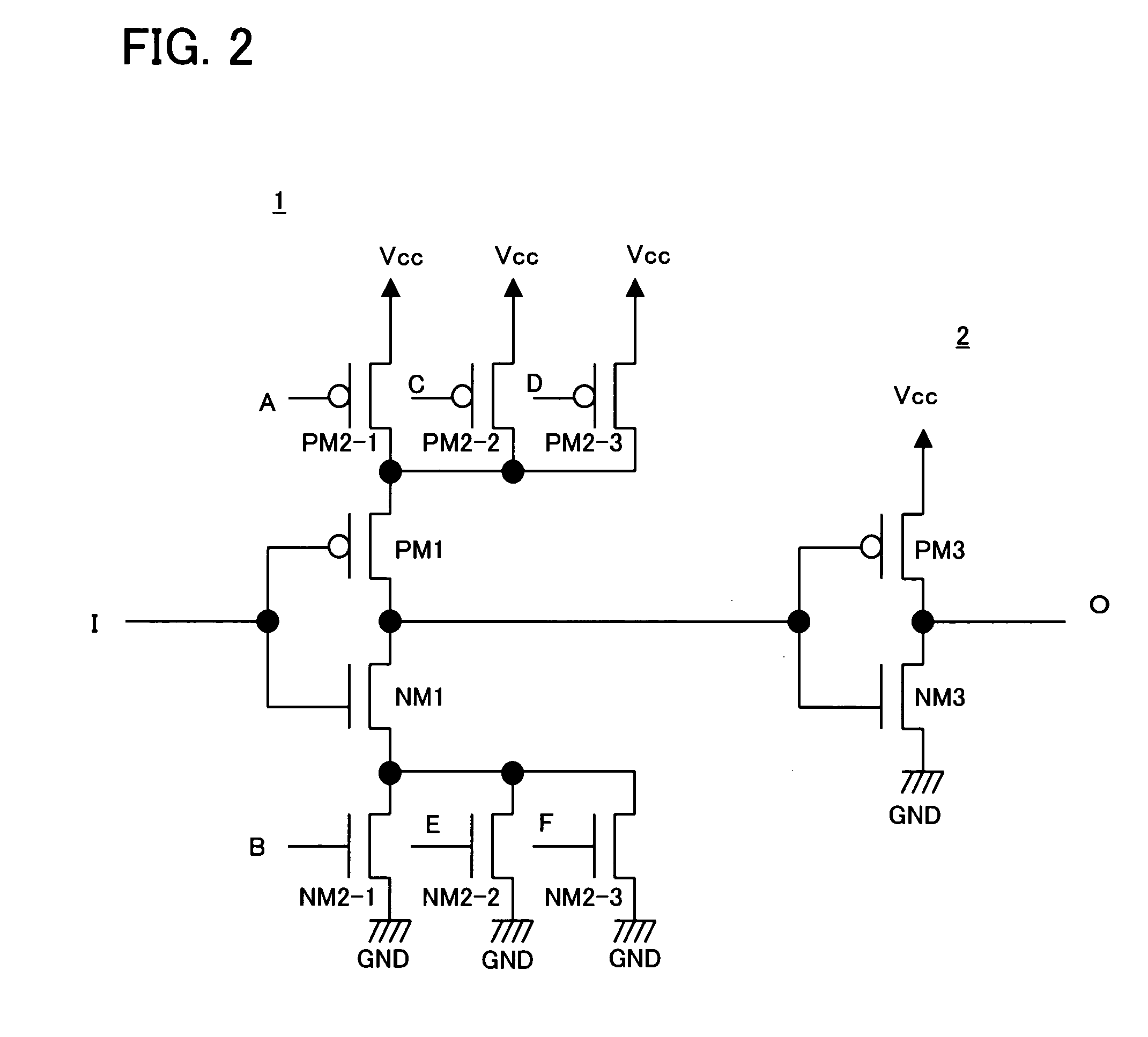
[0038] A preferred embodiment of the present invention will now be described with reference to the accompanying drawings. The delay adjustment circuit of the present invention includes one or more variable resistance devices on a power supply path between an inverter receiving a signal supplied to an input terminal of the delay adjustment circuit and a high potential power supply and / or on a power supply path between the inverter and a low potential power supply. The resistances of the variable resistance devices are varied by control signals to vary the amount of delay. The embodiment of the present invention will now be described in detail. Meanwhile, the following description is directed to delay adjustment in a circuit which latches an address signal of a synchronous semiconductor memory. However, the present invention is not limited to the circuit of latching the address signal, or to a synchronous semiconductor memory, as a matter of course.
[0039]FIG. 1 shows the configuratio...
PUM
 Abstract
Description
Claims
Application Information