Nano-liquid crystal on silicon (LCOS) chip having reduced noise

a liquid crystal and silicon chip technology, applied in the field of semiconductor chip design, can solve the problems of electrical noise electrical cross-talk and/or coupling effect, etc., and achieve the effect of reducing noise and suppressing electrical nois

Active Publication Date: 2007-03-01
WUHAN SPLENDID OPTRONICS TECH +1
View PDF6 Cites 10 Cited by
  • Summary
  • Abstract
  • Description
  • Claims
  • Application Information

AI Technical Summary

Benefits of technology

[0009] The present invention provides an LCoS chip designed to suppress electrical noise that stems from cross-talk between the electrical components of the chip and stray light entered into the chip. The LCoS chip includes multiple polycrystalline layers and metal layers disposed over a silicon substrate and configured to minimize the noise, wherein filling layers are interposed between these layers.

Problems solved by technology

The increases spatial proximity may induce an electrical noise that stems from cell-to-cell cross-talk or coupling effect between the circuit elements.
As a consequence, the major technical challenge in this approach may be how to suppress the electrical cross-talk and / or coupling effect.
As one of the major sources for the voltage leak may be the cross-talk between two neighboring circuit elements and / or cell-to-cell cross talk, the major challenge of this approach would be also how to reduce the electrical cross-talk and / or coupling effect.
The semiconductor chip portion of an LCoS device may have another source of electrical noise: stray light.
The stray light noise may be induced by light unintentionally entered into the chip.

Method used


Image

  • Nano-liquid crystal on silicon (LCOS) chip having reduced noise
  • Nano-liquid crystal on silicon (LCOS) chip having reduced noise
  • Nano-liquid crystal on silicon (LCOS) chip having reduced noise

Examples


Embodiment Construction

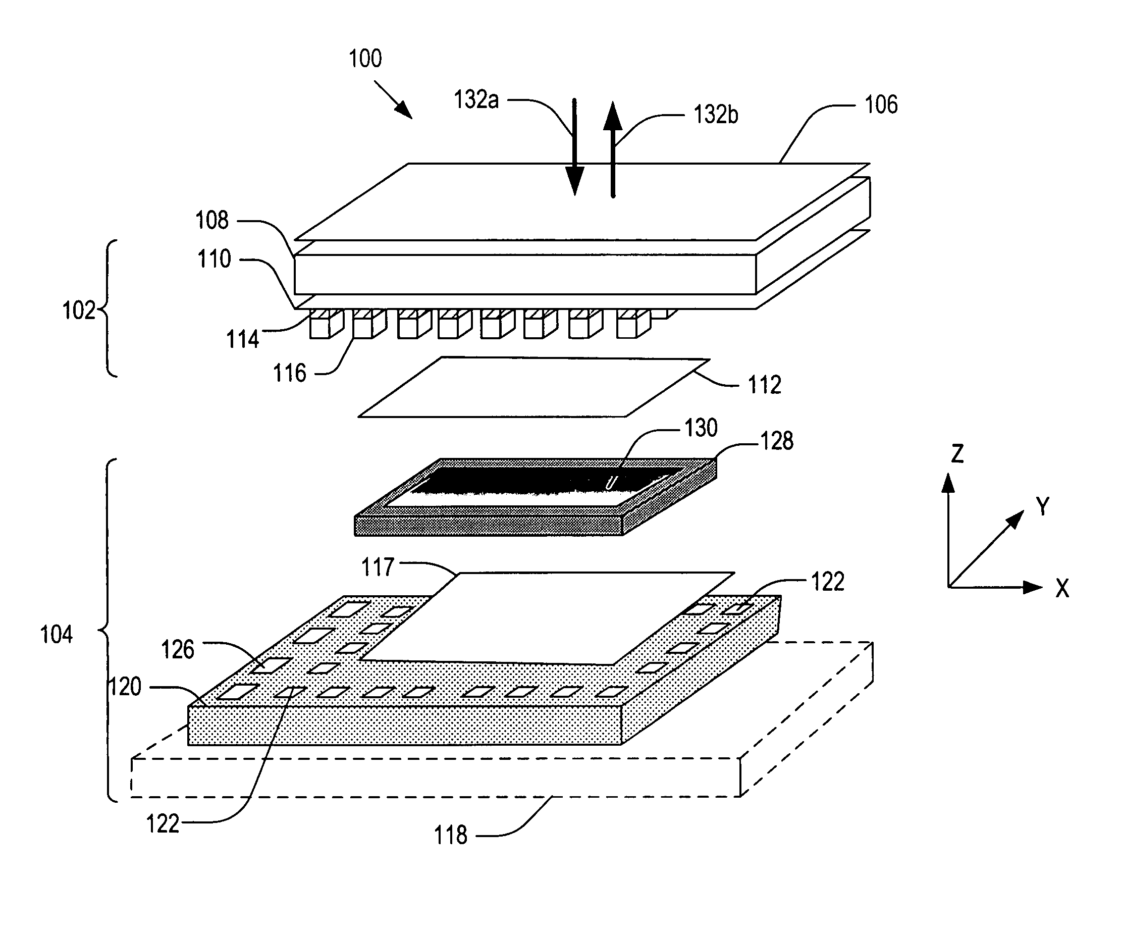
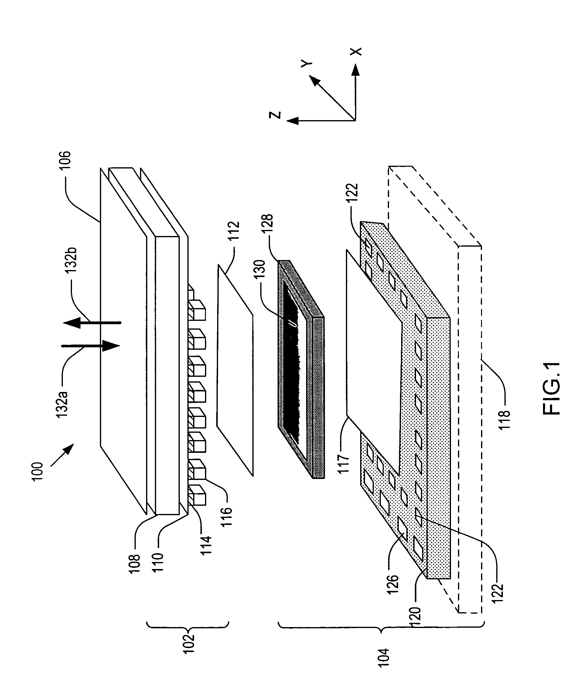
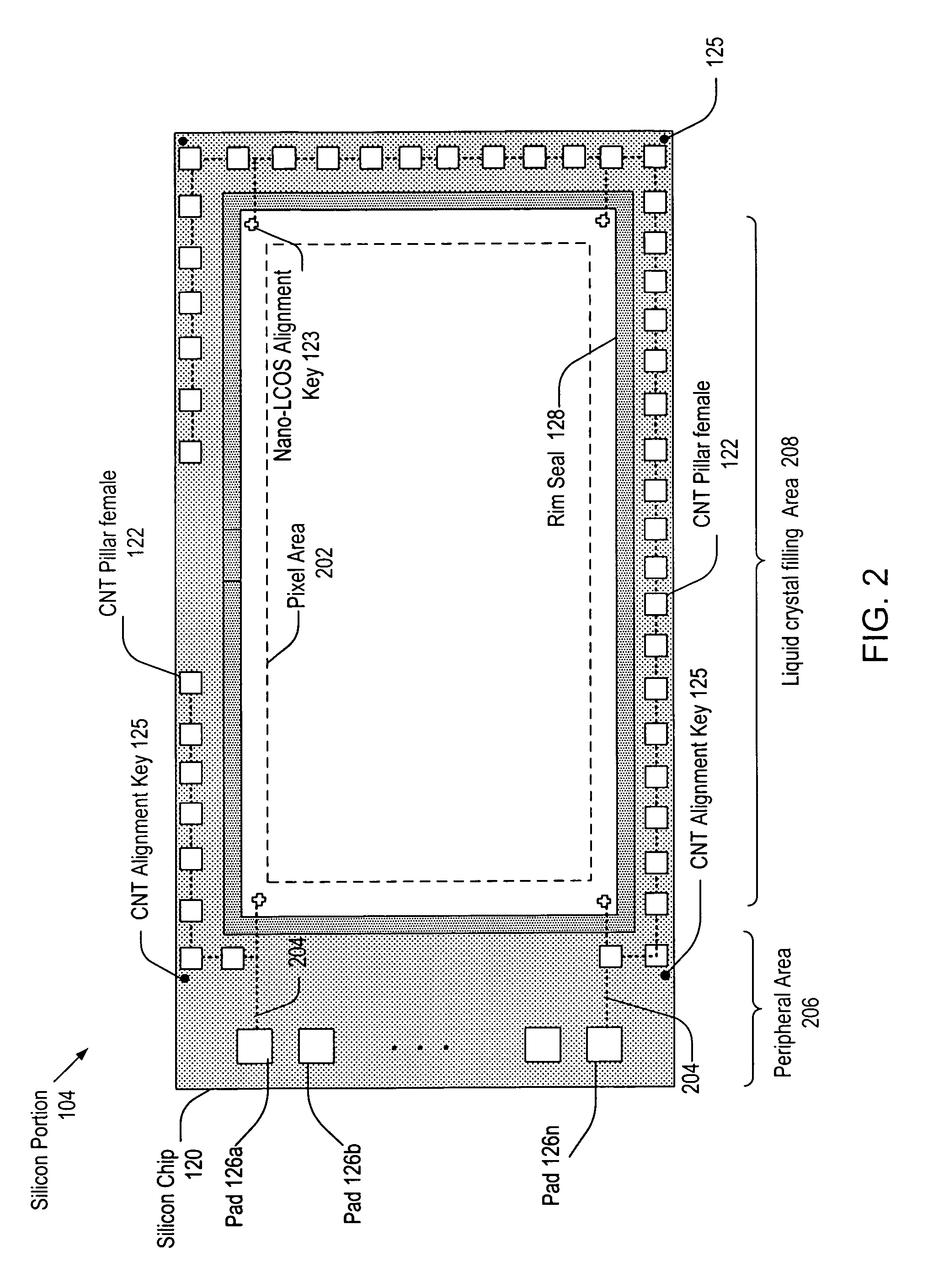
[0024] Referring now to FIG. 1, FIG. 1 is an exploded perspective view of a Nano-LCoS chip shown at 100 according to the present invention. As illustrated, the Nano-LCoS chip may include a glass portion (or equivalently, glass side) 102 and a silicon portion 104. The glass portion 102 may include: a glass 108, preferably made of quartz, fused silica or high temperature glass; an anti-reflection (AR) layer 106 for protecting the glass 108 from mechanical damages and reducing reflection of the incoming light 132a from the top surface of the glass 108; an Indium Tin Oxide (ITO) layer 110; a top inorganic alignment layer 112, preferably made of silicon dioxide, being in contact with liquid crystal 130 and preventing the ITO layer 110 from reacting with the liquid crystal 130; and carbon nanotube (CNT) pillars or columns 116 grown on a metal seed layer 114. In an alternative embodiment, a thin CNT layer with a high level of transparency may be used in place of the ITO layer 110. The thin...


PUM

PropertyMeasurementUnit
peak-to-peak voltage Vppaaaaaaaaaa
electrical potentialsaaaaaaaaaa
brightnessaaaaaaaaaa

Abstract

An LCoS chip designed to suppress electrical noise due to cross-talk between electrical components of the chip and stray light entered into the chip. The LCoS chip includes a silicon substrate having an array of memory cells formed thereon. The chip includes the first polycrystalline silicon layer that forms word lines and a metal layer that forms bit lines, wherein the bit lines are directed orthogonal to the word lines. The chip also includes capacitor storages formed of the second and third second polycrystalline silicon layers. The second polycrystalline layer is disposed over the first polycrystalline silicon layer and over regions of the substrate not covered by the word lines. The metal layer includes shields to reduce cross-talk between neighboring bit lines as well as between the bit lines and capacitor storages. The third polycrystalline layer is configured to reduce cross-talk between the bit lines and word lines.

Description

CROSS REFERENCE TO RELATED APPLICATIONS [0001] This application claims the benefit of U.S. Provisional Application No. 60 / 710,993, entitled “Nano-Liquid Crystal on Silicon (LCoS) Chip Having Reduced Noise,” filed on Aug. 23, 2005, which is incorporated herein by reference in its entirety.FIELD OF THE INVENTION [0002] The present invention relates to semiconductor chip design, and more particularly to design of liquid crystal on silicon (LCoS) cells. BACKGROUND OF THE INVENTION [0003] Micro-display devices having LCoS structures (or, equivalently LCoS devices) are becoming increasingly prevalent in various micro-display applications, such as big-screen TVs, PC monitors, projectors, etc. Typically, an LCoS device has a semiconductor substrate and a liquid crystal positioned on the substrate, where the light passed through the liquid crystal may be magnified by a suitable optical system to display images formed on the liquid crystal for human eyes. [0004] In general, vitally important ...

Claims


Application Information

Patent Timeline
Patent Type & Authority Applications(United States)
IPC IPC(8): G02F1/1339
CPCG02F1/136204G02F2001/136218G02F1/136277G02F1/136213G02F1/136218
Inventor KIM, GIHONGCHUN, TAE SOO
Owner WUHAN SPLENDID OPTRONICS TECH
Why Eureka
Try Eureka