Optical modulator and optical transmission device using same
A light modulator and light modulating technology, which is applied in the direction of instruments, optics, nonlinear optics, etc., can solve the problems of leaking microwave, leaking microwave 2290, and installation position deviation, etc., and achieve good modulation characteristics and the effect of suppressing electrical noise
- Summary
- Abstract
- Description
- Claims
- Application Information
AI Technical Summary
Problems solved by technology
Method used
Image

Examples
no. 1 approach
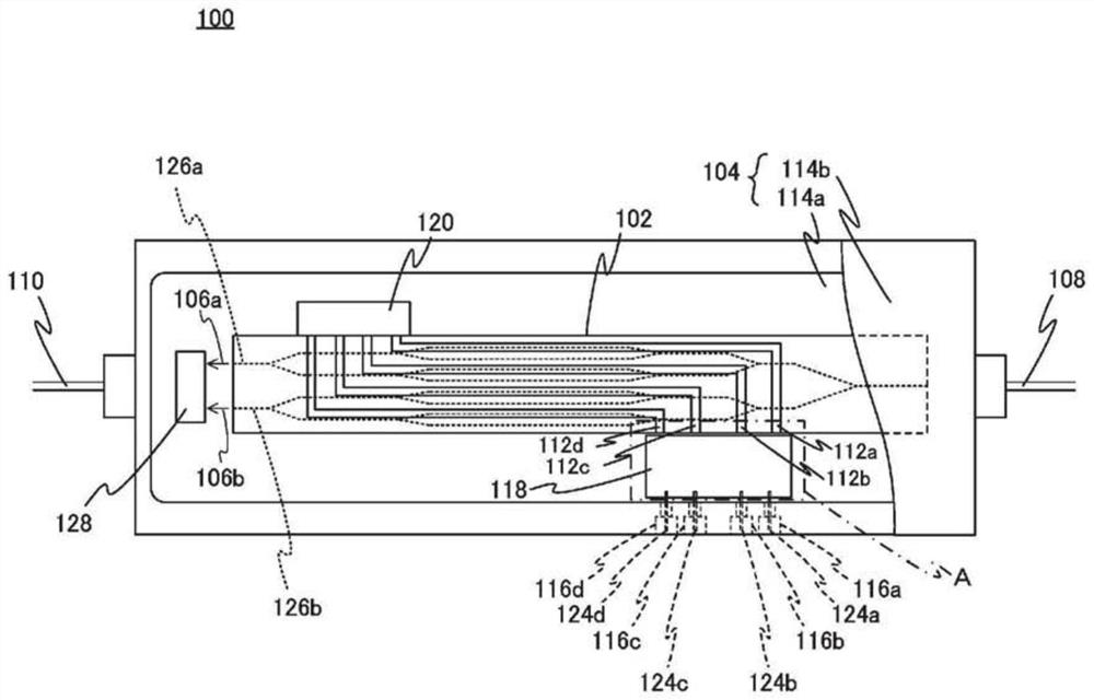
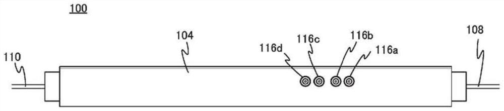
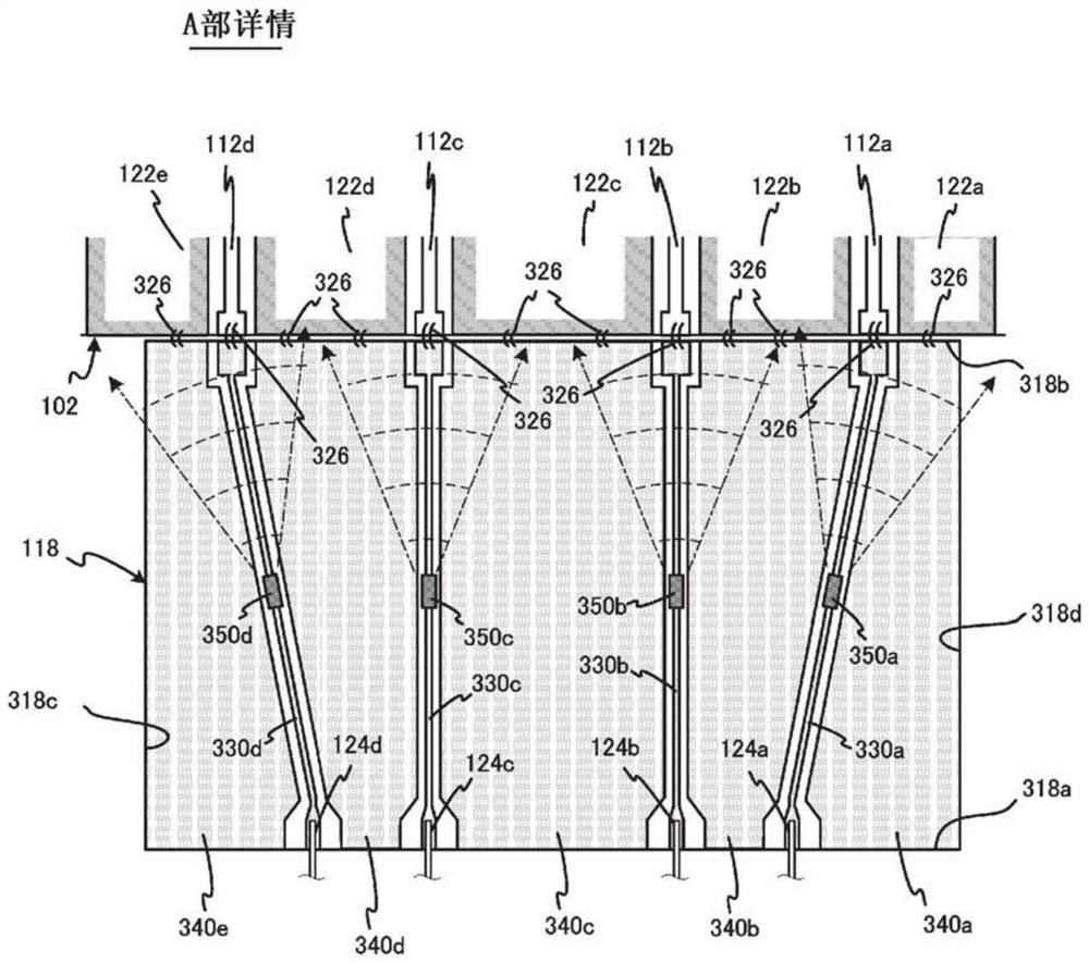
[0059] First, a first embodiment of the present invention will be described. figure 1 is a plan view showing the configuration of the optical modulator 100 according to the first embodiment of the present invention, figure 2 is a side view of the light modulator 100, image 3 yes figure 1 Partial detail view of part A in .
[0060] The light modulator 100 includes a light modulation element 102, a case 104 for accommodating the light modulation element 102, an input optical fiber 108 for making light incident on the light modulation element 102, and a light output from the light modulation element 102 to the outside of the case 104. Guided output fiber 110 .
[0061] The optical modulation element 102 is a DP-QPSK modulator for optical modulation of, for example, 400 Gb / s, and is composed of two nested Mach-Zehnder optical waveguides disposed on, for example, an LN substrate, each nested Mach-Zehnder The optical waveguides respectively include two Mach-Zehnder type opti...
no. 2 approach
[0132] Next, an optical modulator according to a second embodiment of the present invention will be described. In the above-mentioned optical modulator 100 of the first embodiment, the arrangement pitch of the signal electrodes 112 of the light modulation element 102 is equal to the arrangement pitch of the signal input terminals 124 , but the present invention is not limited thereto. The arrangement pitch of the signal electrodes of the light modulation element may be larger than the arrangement pitch of the signal input terminals 124 , or may be smaller than the arrangement pitch of the signal input terminals 124 . This embodiment is the first example in which the arrangement pitch of the signal electrodes of the optical modulation element is smaller than the arrangement pitch of the signal input terminals 124 .
[0133] Figure 8 is a plan view showing the configuration of the light modulator 800 according to the second embodiment of the present invention, Figure 9 yes ...
no. 3 approach
[0153] Next, an optical modulator according to a third embodiment of the present invention will be described. In the interposer substrates 118 , 418 , 518 , 618 , and 718 of the above-mentioned first embodiment and its modifications, and the interposer substrate 918 of the second embodiment, the signal conductor pattern 330 and the like and 940 are configured as shapes including bends. , but, of course, the present invention is not limited to such a bent shape. These signal conductor patterns 330 and 940 may be formed using curves instead of bending.
[0154] This embodiment is a second example in which the arrangement pitch of the signal electrodes of the optical modulation element is smaller than the arrangement pitch of the signal input terminals 124. In particular, as will be described later, the signal conductor patterns 1130a, 1130b, 1130c, and 1130d of the relay substrate 1018 The curved portion is formed of a curved line without being bent.
[0155] Figure 10 is a ...
PUM
 Abstract
Description
Claims
Application Information