High speed operation method for twin MONOS metal bit array

a metal bit array and high-speed operation technology, applied in the field of nonvolatile memory cells with twin monos structure, can solve the problem of area penalty of stitching area, and achieve the effect of saving memory cell area, and eliminating the set up time for the control gate voltag

Active Publication Date: 2007-03-01
HALO LSI INC
View PDF22 Cites 30 Cited by
  • Summary
  • Abstract
  • Description
  • Claims
  • Application Information

AI Technical Summary

Benefits of technology

[0013] In a first embodiment of the present invention, the alternative control gates are set at the same voltage. For example, odd numbered control gates are set at the override voltage 3.3V and even numbered control gates are set at the select voltage 1.8V. The memory cells under the even numbered control gates set at the select voltage 1.8V can be accessible. Assembly of the cells under the even numbered control gates can be the virtual bank called “even bank”. In the case that odd numbered control gates are set at the select voltage and even numbered control gates are set at the override voltage, the cells under the odd numbered control gates are accessible. Assembly of the cells under the odd numbered control gates can be a virtual bank called “odd bank”. In the present invention, the operation cycle time can be smaller than that of the prior art as long as the cells within the same virtual bank are selected. That is because the set up time for the control gate voltage can be eliminated. However, in case of switching from one virtual bank to another one, there will be an additional access time hit because control gate voltages (select, over-ride) need to be switched. That means the memory array in the present invention is characterized by 2 different access times. This could require system level optimization to take full adv

Problems solved by technology

For the reason above, an operational method to reduce or eliminate the factor of the control gate is an important issue for h

Method used


Image

  • High speed operation method for twin MONOS metal bit array
  • High speed operation method for twin MONOS metal bit array
  • High speed operation method for twin MONOS metal bit array

Examples


first embodiment

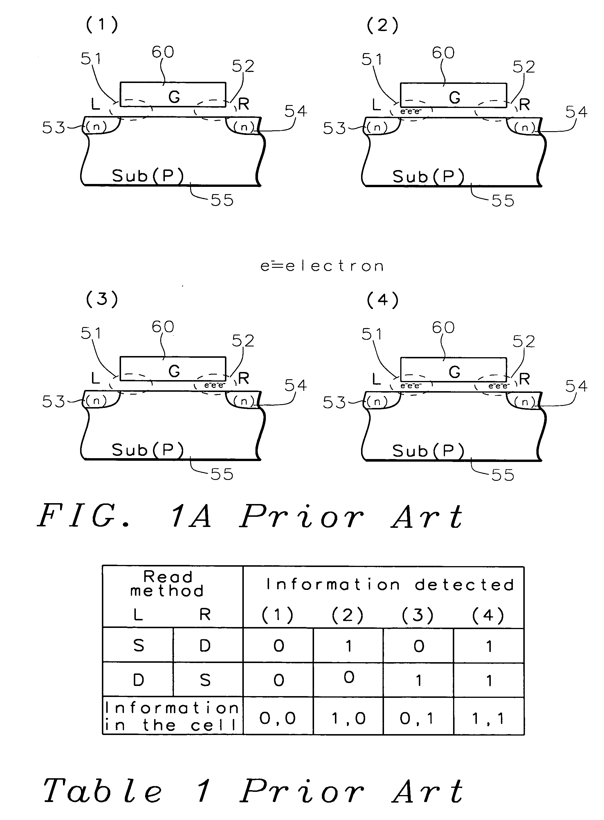
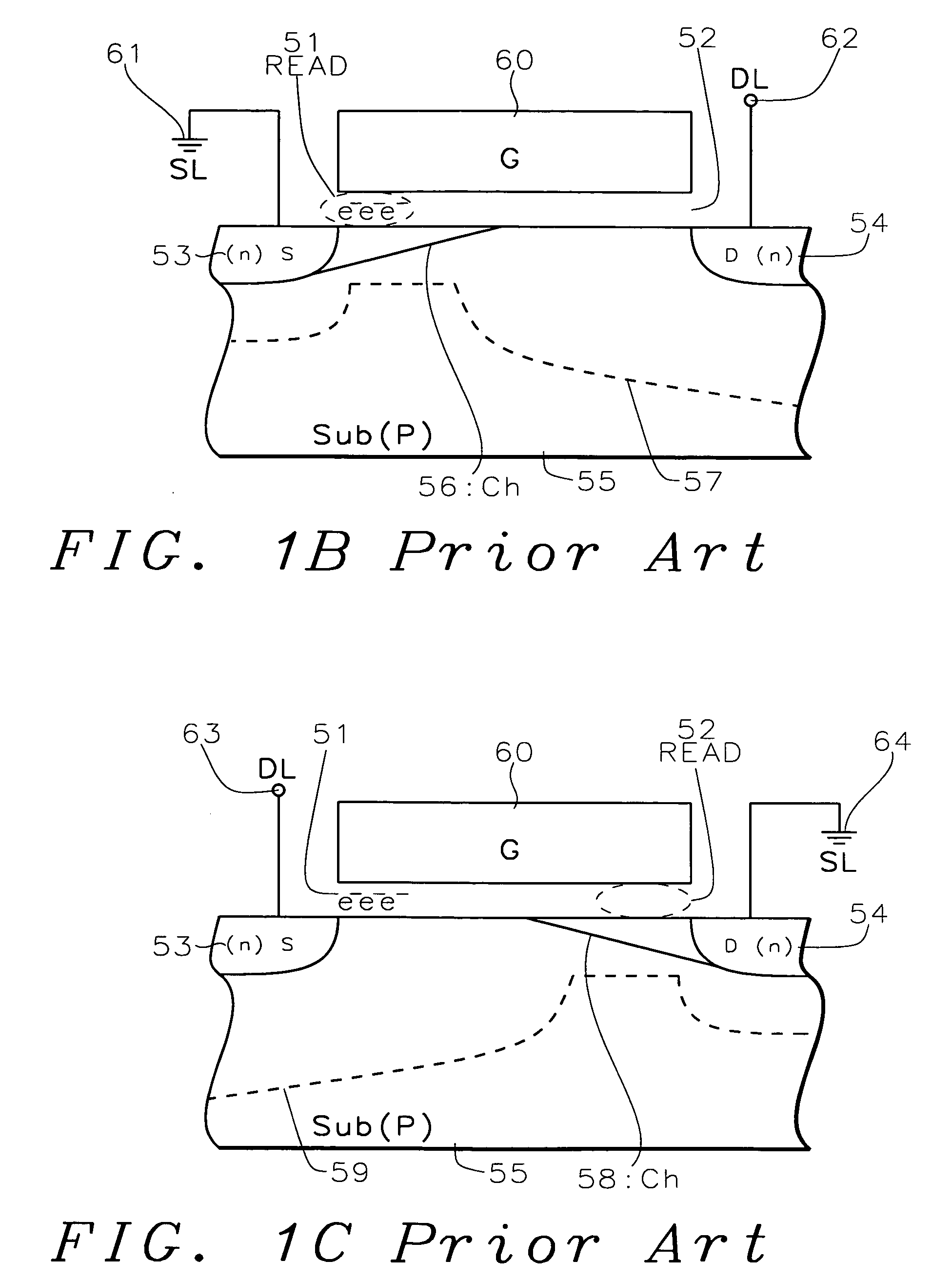
[0039] In the present FIG. 13 shows the read operation voltage condition in a twin MONOS memory array 1. The selected cell 217 is supposed to be read. The cell 218 under the selected control gate CG2> is not selected. In FIG. 13, the even numbered control gates are set at the select voltage 1.8V and the odd numbered control gates are set at the override voltage 3.3V at the beginning of the read mode. The assembly of the cells under the even numbered control gate can be thought of as virtual “even bank”5. The assembly of the cells under the odd numbered control gate can be thought of as virtual “odd bank”4. The selected bit line BL3> is precharged at 1.8V before the selected word gate WL1> is turned on. The unselected bit lines are set at 0V. After the selected bit line BL3> is precharged at 1.8V, the selected word gate WL1> is set at 2V. The unselected WL's are set at 0V. The voltage level of the selected Bit line BL3> is detected by a sense amplifier after the selected word gate WL...

second embodiment

[0048] Though the high enough override CG voltage is used for override in the prior art shown in FIG. 16, another override method is used in the present invention shown in FIG. 17A. In the present invention, 2.5V is applied to both CGs 23 and 25. That is, override voltage is eliminated. That is as if all the control gates were connected together as shown in FIG. 17B. However, the word gate voltage can be applied independently of the control gate voltage. This condition is achieved electrically by applying the same voltage to all the control gates. The BL at the override side is set at 1.5V (not precharge) and the BL at the select side is set at 0V. After the CG voltage and BL voltage are set, WL is set at 2.0V. In the present invention, DIBL (Drain Induced Barrier Lowering) is utilized for override. Because the Vth of the override CG 23 is lowered enough by DIBL owing to the bit line voltage (1.5V), the read operation for the selected cell 21 can be done without error. In the presen...

third embodiment

[0056]FIGS. 22-25 show high-speed memory operation method using metal bit twin MONOS array where a pair of storage area regions hold complementary bits. Hereinafter, this method is called “complementary method”.

[0057]FIG. 22 shows the voltage condition of program operation in the complementary method where complementary memory cell 301 comprised of a pair of complementary bits is programmed. In the complementary method, one cell of the complementary memory cell 301 is programmed at data “0” and another one cell of the complementary memory cell 301 is programmed at data “1”. The programming of data “0” or inhibition of program (data “1”) is as described in the prior art of non-complementary method utilizing twin MONOS memory device.

[0058] To program data “0” in the left cell 310 and data “1” in the right cell 311, BL1> is set at 0V, BL2> is set at 4.5V and BL3> is set at 1.8V. 4.5V of BL2>is the BL program voltage and 1.8V of BL3> is program inhibit voltage. Select control gate CG2>...


PUM


Abstract

The present invention provides a novel operational method of twin MONOS metal bit or diffusion bit structure for high-speed application. In a first embodiment of the present invention, the alternative control gates are set at the same voltage. In a second embodiment of the present invention, all the control gates are set at the operational voltage from the beginning. In both embodiments, the bit line and word gate are used to address the selected memory cell.

Description

BACKGROUND OF THE INVENTION [0001] 1) Field of the Invention [0002] The Invention relates to a non-volatile memory cell with Twin MONOS structure, particularly aiming to high-speed application. [0003] 2) Description of the Related Art [0004] Ishii et al. introduced the semiconductor memory element and its operation method in JP60200566 wherein two trap sites 51 and 52 exist in the insulator film underneath the gate polysilicon layer as shown in prior art FIG. 1A. The electron can be trapped in each trap site 51 and 52 as shown in FIG. 1A (1)-(4). [0005] In FIG. 1B, the method to detect the data status of the trap site 51 is shown. Gate 60 is set at high level (typically higher than 1V, hereinafter it is called “H” level) and select line SL 61 is set at low level (hereinafter it is called “L” level) e.g. ground level. And the data line DL 62 is set at “H” level. Vth over the channel region 56 is high because the electrons exist at the trap site 51. Therefore, the MOSFET does not cond...

Claims


Application Information

Patent Timeline
IPC IPC(8): G11C16/04
CPCG11C16/0475
Inventor OGURA, TOMOKOOGURA, NORIOGURA, SEIKISAITO, TOMOYABABA, YOSHITAKA
Owner HALO LSI INC
Why Eureka
Try Eureka