

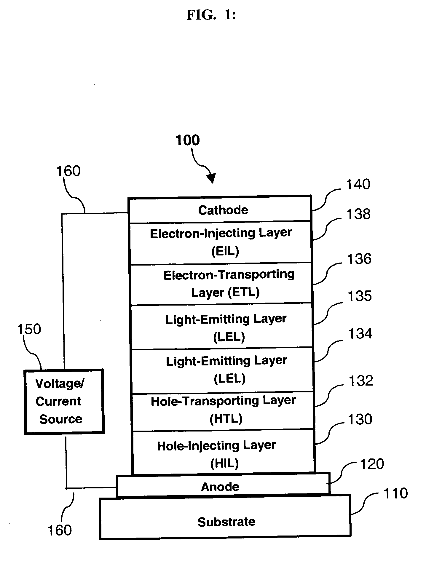
Electron-transporting layer for white OLED device
a technology of electric transport layer and white oled, which is applied in the direction of discharge tube luminescnet screen, discharge tube/lamp details, natural mineral layered products, etc., can solve the problems of inferior stability, short lifetime, and higher drive voltage, and achieves lower operating voltage, better stability, and lower operating voltage
- Summary
- Abstract
- Description
- Claims
- Application Information
AI Technical Summary
Benefits of technology
Problems solved by technology
Method used
Image

Examples
example 4 (
Inventive)
[0243] An inventive OLED device was constructed as in Example 1, except that in step 6 the layer was a 50:50 mixture of BPhen and Compound C-8 doped with 1% lithium metal.
example 5 (
Inventive)
[0244] An inventive OLED device was constructed as in Example 1, except that in step 6 the layer was a 50:50 mixture of BPhen and Compound C-8 doped with 2% lithium metal.
examples 1-5
Results (Examples 1-5)
[0245] The devices were tested by applying a current across the electrodes of 20 mA / cm2 and measuring the spectrum and required drive voltage. The relative luminous efficiency is defined as the luminous efficiency of the example device, in cd / A, divided by the luminous efficiency in, cd / A, of reference Example 1. The CIE change magnitude is the magnitude of the color change in CIE color space relative to reference Example 1. The following table shows the results.
TABLE 1Example:12345TypeCompCompCompInvInv(Inventive or Comparative)Drive voltage at 20 mA / cm25.804.406.404.404.50Relative Drive voltage1.000.761.100.760.78Yield (cd / A)8.9011.50 5.0610.709.93Relative Luminous Efficiency1.001.290.571.201.12CIE x0.310.370.320.340.34CIE y0.330.380.330.350.35CIE change magnitude—0.080.010.040.04
LUMO Values.
[0246] An important relationship exists when selecting the first compound(s) and second compound(s) of the invention. A comparison of the LUMO values of the first and...
PUM
| Property | Measurement | Unit |
|---|---|---|
| work function | aaaaa | aaaaa |
| drive voltages | aaaaa | aaaaa |
| drive voltages | aaaaa | aaaaa |
Abstract
Description
Claims
Application Information