Dual-gate dynamic random access memory device having vertical channel transistors and method of fabricating the same

a dynamic random access memory and vertical channel transistor technology, applied in the field of dynamic random access memory devices having vertical channel transistors, can solve the problems of increasing the integration density of semiconductor devices, increasing the difficulty of ensuring sufficient electrostatic capacitance, and reducing the retention time, so as to achieve high layout efficiency

Active Publication Date: 2007-03-08
SAMSUNG ELECTRONICS CO LTD
View PDF3 Cites 64 Cited by
  • Summary
  • Abstract
  • Description
  • Claims
  • Application Information

AI Technical Summary

Benefits of technology

[0007] The invention is directed to a D

Problems solved by technology

There are arising various technical problems along with an increase in integration density of semiconductor devices.
I particular, the shrinking-down of DRAMs in dimension makes it more difficult to assure sufficient electrostatic capacitance.
However, increasing impurity concentration in the channel is accompanied by an increase of leakage current, resulting in a decrea

Method used


Image

  • Dual-gate dynamic random access memory device having vertical channel transistors and method of fabricating the same
  • Dual-gate dynamic random access memory device having vertical channel transistors and method of fabricating the same
  • Dual-gate dynamic random access memory device having vertical channel transistors and method of fabricating the same

Examples


first embodiment

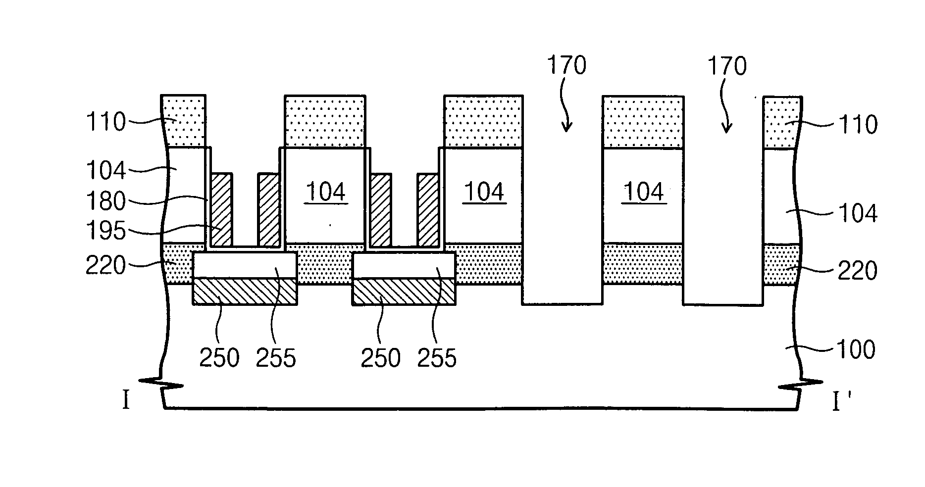
[0072] Referring to FIGS. 9A through 9C, the gate insulation films 180 and the word lines 195 are formed on the inner walls of the first trenches 120. The gate insulation films 180 and the word lines 195 may be completed by the same steps as those of the first embodiment or the modifications thereof. In this embodiment, the gate insulation films 180 may be formed all over inner walls of the first trenches 120.

[0073] Before forming the gate insulation films 180 or after forming the word lines 195, the lower impurity regions 220 are formed under the active regions 102. As in the first embodiment, the lower impurity regions 220 are used as the source regions of the transistors. The procedure of forming the lower impurity regions 220 is the same as that of the first embodiment.

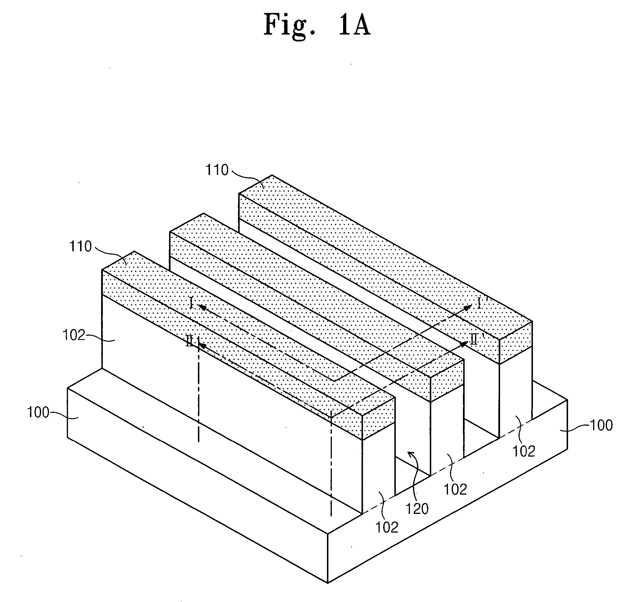
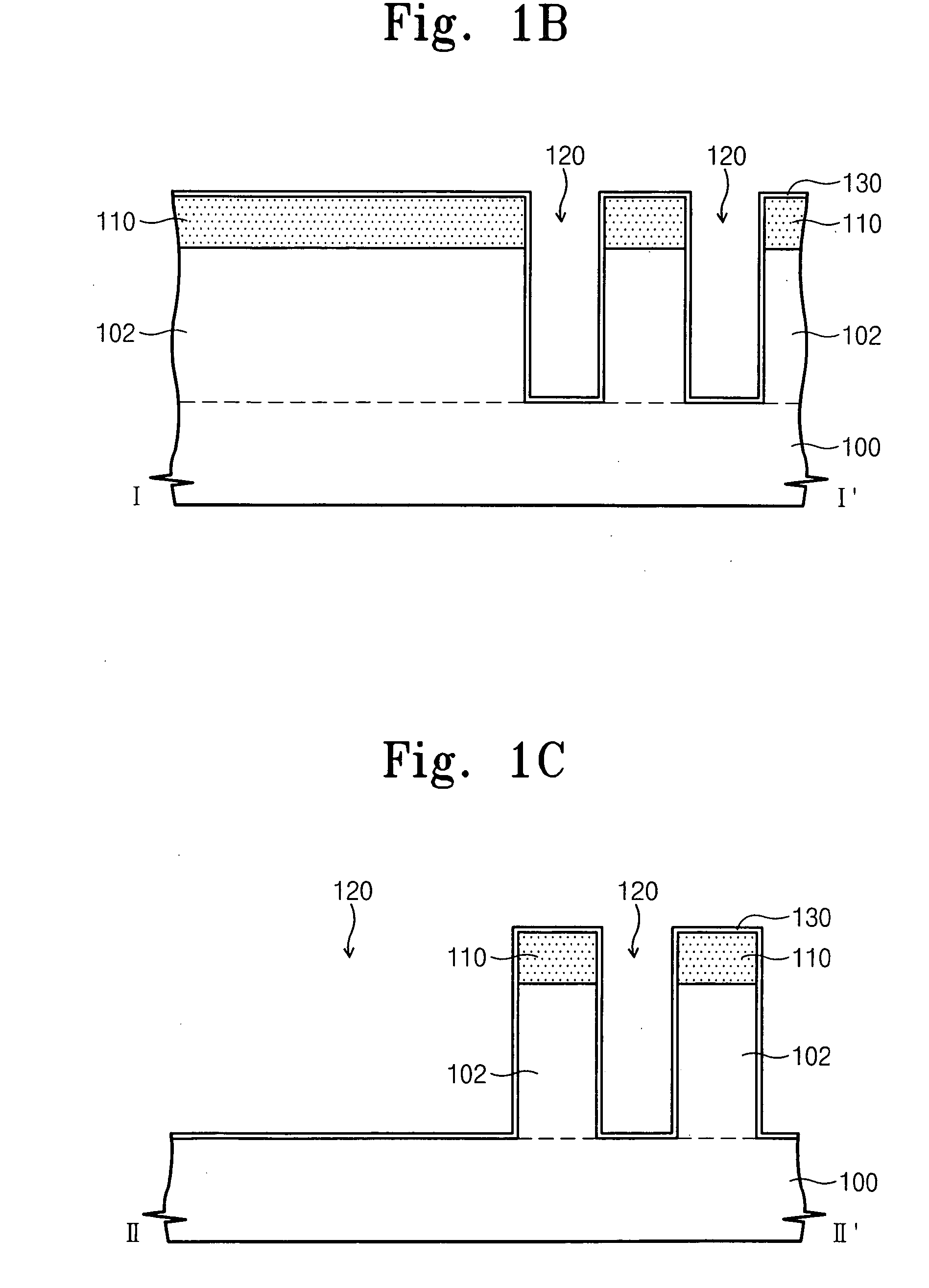
[0074] Referring to FIGS. 10A through 10C, the first insulation film is deposited on the resultant structure including the word lines 195 and then eroded to be flattened until exposing the first mask patterns 110...

second embodiment

[0082] Referring to FIGS. 13B and 13C, after forming the first trenches 120 on the conductive patterns 250, the gate insulation films 180 and the word lines 195 are formed in the first trenches 120. The steps of forming the first trenches 120, the gate insulation films 180, and the word lines 195 are as same with those of the During this, as the first trenches 120 are formed on the conductive patterns 250, the discontinuous interfaced 99 are removed therefrom. Therefore, there is no influence on characteristics of transistors by the discontinuous interfaces 99.

[0083] According to another embodiment, as shown in FIGS. 14A and 14B, the bottom surfaces of the first trenches 120 may be separated from the conductive patterns 250. That is, the epitaxial layer 101 may be interposed between the first trenches 120 and the conductive patterns 250.

[0084] According to the embodiments of the invention, the conductive patterns 250 are used as the source regions of the transistors. With this con...


PUM


Abstract

A dynamic random access memory (DRAM) device has dual-gate vertical channel transistors. The device is comprised of pillar-shaped active patterns including source regions contacting with a semiconductor substrate, drain regions formed over the drain regions, and channel regions formed between the source and drain regions. The active patterns are disposed in a cell array field. On the active patterns, bit lines are arranged to connect the drain regions along a direction. Between the active patterns, word lines are arranged intersecting the bit lines. Gat insulation films are interposed between the word lines and active patterns.

Description

CROSS-REFERENCE TO RELATED APPLICATIONS [0001] This U.S. non-provisional patent application claims priority under 35 U.S.C. § 119 of Korean Patent Application 2005-81896 filed in the Korean Intellectual Property Office on Sept. 2, 2005, the entire contents of which are hereby incorporated by reference. BACKGROUND [0002] The subject matter described herein is concerned with semiconductor devices and methods for fabricating the same. In particular, the subject matter described herein relates to a dynamic random access memory (DRAM) device having dual-gate vertical channel transistors and a method of fabricating the same. [0003] A unit cell of a general semiconductor memory device is comprised of a single transistor and information storage. For example, a DRAM unit cell has a single capacitor as the information storage, while a flash memory unit cell has a floating gate. A static RAM cell uses a flip-flop circuit as the information storage. [0004] There are arising various technical pr...

Claims


Application Information

Patent Timeline
IPC IPC(8): H01L29/94
CPCH01L27/108H01L27/10802H01L27/10891H01L27/10885H01L27/10844H10B12/20H10B12/01H10B12/488H10B12/00H10B12/482H10B99/00
Inventor SONG, KI-WHANLEE, JONG-DUKPARK, BYUNG-GOOKJEONG, HOON
Owner SAMSUNG ELECTRONICS CO LTD
Why Eureka
Try Eureka