Semiconductor device, method of manufacturing the same, circuit board, and method of manufacturing the same

Active Publication Date: 2007-03-08
SEMICON COMPONENTS IND LLC
View PDF12 Cites 69 Cited by
  • Summary
  • Abstract
  • Description
  • Claims
  • Application Information

AI Technical Summary

Benefits of technology

[0013] The present invention has been made in view of the problems described above. A main object of the present invention is to provide a semiconductor device having improved connection reliability against external force such as

Problems solved by technology

This causes a problem that an area necessary for mounting the semiconductor element is increased.
The thermal stress results in a problem that a crack is generated in the solder bumps, thereby reducing connection reliability of the semiconductor element.
Accordingly, bonding strength between the ele

Method used


Image

  • Semiconductor device, method of manufacturing the same, circuit board, and method of manufacturing the same
  • Semiconductor device, method of manufacturing the same, circuit board, and method of manufacturing the same
  • Semiconductor device, method of manufacturing the same, circuit board, and method of manufacturing the same

Examples


Example

[First Embodiment]

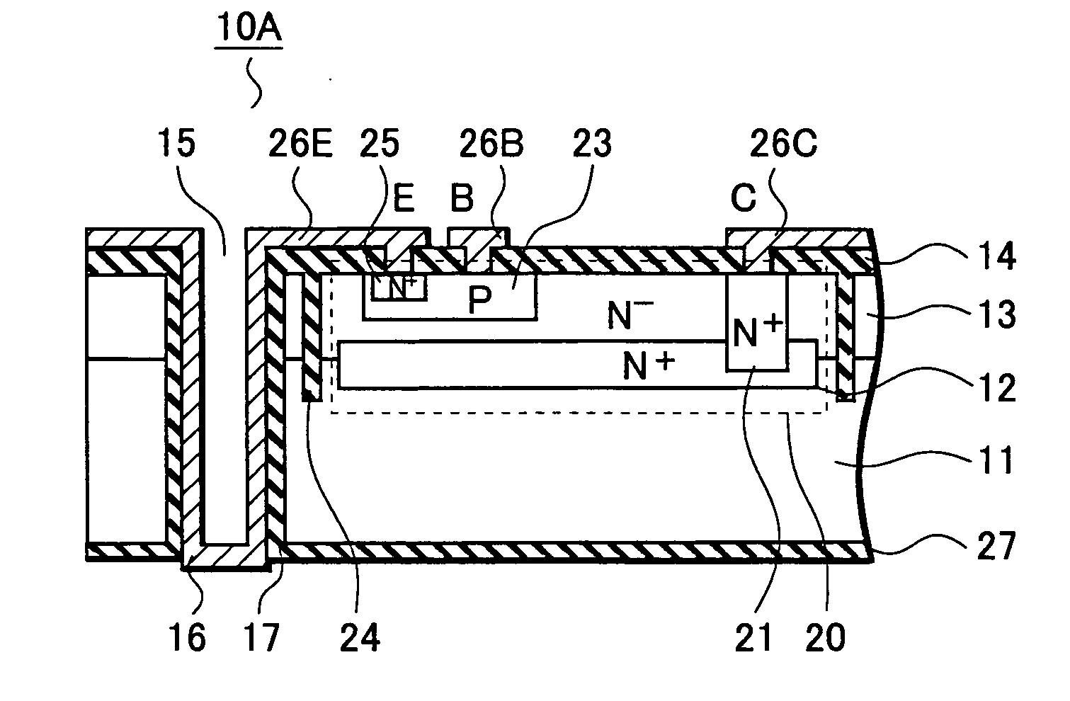
[0027] By referring to FIGS. 1A to 3, a configuration of a semiconductor device of a first embodiment will be described.

[0028] As illustrated in a cross sectional view of FIG. 1A, in a semiconductor device 10A of this embodiment includes, an active region 20 is formed in an upper surface (first main surface) of a semiconductor substrate 11, and is surrounded by a trench 24 filled with an oxide. A through-hole electrode 16 electrically connected to the active region 20 extends from the upper surface of the semiconductor substrate 11 to a lower surface (second main surface) of the semiconductor substrate 11. A bottom end of the through-hole electrode 16 downwardly juts out of an insulating film 27 covering the lower surface of the semiconductor substrate 11.

[0029] Generally, the active region 20 is a region where an active element such as a transistor or a diode is formed. In this embodiment, a bipolar transistor is formed in the active region 20. A MOSFET, an IC,...

Example

[Second Embodiment]

[0050] In a second embodiment, by referring to FIGS. 4A to 5B, descriptions will be provided for a method of manufacturing the semiconductor device 10A illustrated in FIG. 1A.

[0051] By referring to FIG. 4A, first, an active region 20 including a bipolar transistor is formed in an upper surface of a p type semiconductor substrate 11 having a thickness of approximately 600 μm.

[0052] A method of manufacturing the active region 20 is as follows. First, an n+ type buried layer 12 is provided in the upper surface of the semiconductor substrate 11 by ion implantation. Subsequently, an n− epitaxial layer 13 is formed on the upper surface of the semiconductor substrate 11. The epitaxial layer 13 has a thickness of approximately 1.5 μm. Thereafter, a collector contact region 21, a base region 23 and an emitter region 29 are formed by ion implantation. The collector contact region 21 is formed to reach the buried layer 12 by adopting phosphorus ions (P) as an ion species ...

Example

[Third Embodiment]

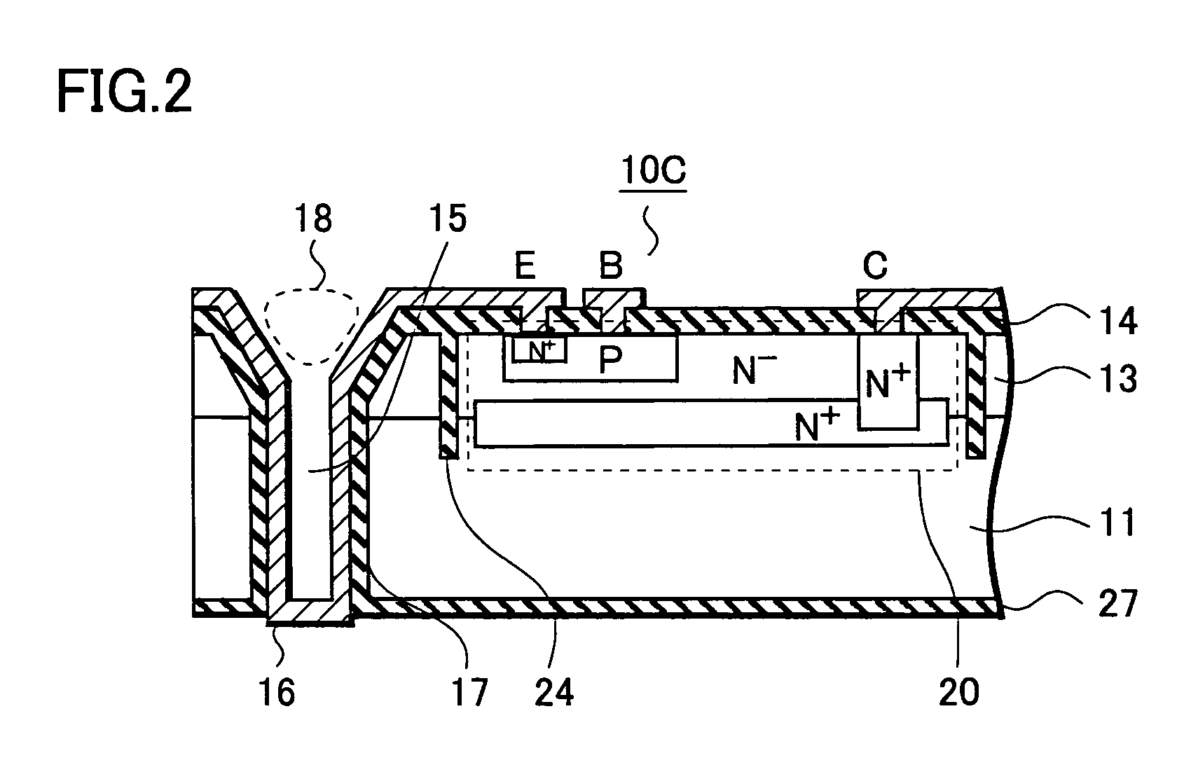
[0068] In a third embodiment, by referring to FIGS. 6A to 6D, descriptions will be provided for a method of manufacturing the semiconductor device 10B having a structure shown in FIG. 1B. The manufacturing method of this embodiment is basically similar to that of the second embodiment described above, and it is a different point that a concave portion 28 is provided to each through hole. Hereinafter, the manufacturing method will be described, focusing on this point.

[0069] By referring to FIG. 6A, an active region 20 is provided in a surface of a semiconductor substrate 11, and then, through holes 15 are formed to pass through a group including the semiconductor substrate 11 and layers stacked on the semiconductor substrate 11. In this embodiment, the concave portion 28 is formed in a bottom end of each of the through holes 15, the bottom end being the lowermost portion of the semiconductor substrate 11. In the bottom end of each of the through holes 15, the conc...


PUM


Abstract

In the semiconductor device of the present invention, an active region is formed in an upper surface of a semiconductor substrate, and is surrounded by a trench filled with an oxide. A through-hole electrode electrically connected to the active region extends from the upper surface of the semiconductor substrate to a lower surface thereof. A bottom end of the through-hole electrode juts out of an insulating film covering the lower surface of the semiconductor substrate. Accordingly, a jutting portion of the through-hole electrode is embedded in the bonding material when the semiconductor device is mounted on a mounting board, and thus the connection reliability therebetween is improved.

Description

[0001] Priority is claimed to Japanese Patent Application Number JP2005-252186 field on Aug. 31, 2005, the disclosure of which is incorporated herein by reference in its entirety. BACKGROUND OF THE INVENTION [0002] 1. Field of the Invention [0003] The present invention relates to a semiconductor device including a through-hole electrode passing through a semiconductor substrate, and a method of manufacturing the same. In addition, the present invention relates to a circuit board including a through-hole electrode passing through a semiconductor substrate and a method of manufacturing the same. [0004] 2. Description of the Related Art [0005] A circuit device is conventionally formed, for instance, by mounting a semiconductor element, such as an IC chip, on a mounting board having a surface on which conductive paths are formed. There are two types of mounting configurations, which are face-up mounting and face-down mounting (flip chip technique), as methods for connecting the conducti...

Claims


Application Information

Patent Timeline
IPC IPC(8): H01L27/082H01L21/331
CPCH01L21/76898H01L23/481H01L2924/1305H01L25/0657H01L25/50H01L29/66265H01L29/7317H01L2224/16H01L2225/06513H01L2225/06524H01L2225/06541H01L2924/01078H01L2924/04941H01L2924/3025H01L2924/13091H01L2924/00H01L21/77H01L23/48H01L25/00
Inventor UMEMOTO, MITSUO
Owner SEMICON COMPONENTS IND LLC
Why Eureka
Try Eureka