Multilayer anisotropic conductive adhesive and connection structure using the same

a technology of anisotropic conductive adhesives and connection structures, applied in the direction of film/foil adhesives without carriers, film/foil adhesives, transportation and packaging, etc., can solve problems such as reflow resistance, and achieve the effect of excellent resistance reflow

Inactive Publication Date: 2007-03-08
SONY CORP +1
View PDF7 Cites 27 Cited by
  • Summary
  • Abstract
  • Description
  • Claims
  • Application Information

AI Technical Summary

Benefits of technology

[0016] It is assumed that the exothermic peak temperature is higher than an exothermic peak temperature of the past, which is lower than 130° C., and so hardening in the thermocompression may progress slowly in the reflow treatment to easily follow the expansion of electronic components connected.
[0019] Accordingly, with the first adhesive layer facing the side of electronic components, where exfoliation tends to occur after reflow treatment, to obtain favorable reflow resistance, and with the second adhesive layer being disposed on the opposite side or in the middle and using, for example, typically-used relatively inexpensive material for the second adhesive layer, the cost as a whole can be reduced.
[0028] With the above materials being used for the hardening agent, reflow resistance can further be improved.
[0032] According to the composition of the above-described connection structure of the present invention, since the first electronic component which has an electrode and an insulating film on the surface thereof and the second electronic component which has an electrode on the surface thereof are electrically connected through the above-described multilayer anisotropic conductive adhesive of the present invention, at least the DSC exothermic peak temperature of the top adhesive layer or bottom adhesive layer is 130° C. or more and 180° C. or less, and such a characteristic that the top adhesive layer or bottom adhesive layer does not easily exfoliate after reflow treatment is obtained; and therefore with this adhesive layer not easily exfoliating being disposed to face the side of electronic components where exfoliation tends to occur after reflow treatment, favorable reflow resistance can be obtained.
[0038] According to the above-described present invention, since the multilayer anisotropic conductive adhesive has an adhesive layer whose DSC exothermic peak temperature is 130° C. or more and 180° C. or less, a connective material (adhesive) and a connection structure with excellent resistance reflow can be obtained, which has been difficult to be obtained in a conventional connective material.

Problems solved by technology

However, regarding ACFs and NCFs in related art, there has been a problem with this reflow resistance.

Method used


Image

  • Multilayer anisotropic conductive adhesive and connection structure using the same

Examples


example 1

Practice Example 1

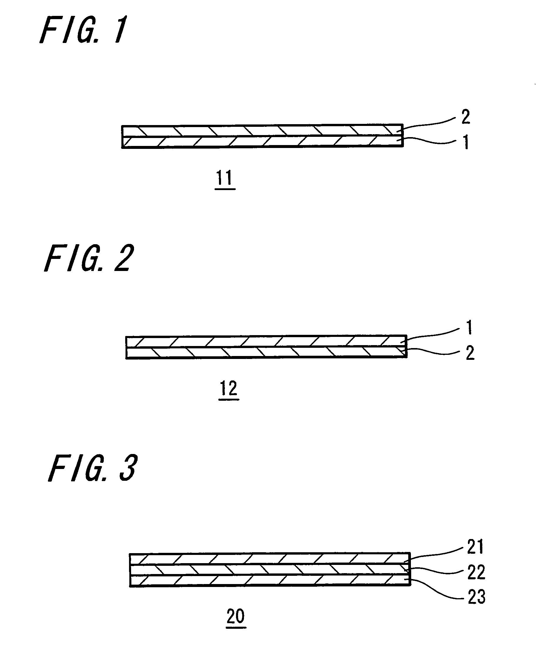
[0083] As a first adhesive layer the film 2 of 40 μm in thickness whose DSC exothermic peak temperature is 151° C. was given and as a second adhesive layer the film 5 of 10 μm in thickness whose DSC exothermic peak temperature is 121° C. was given; and a multilayer anisotropic conductive adhesive of two-layer structure was formed by laminating these layers.

[0084] Specifically, after coating liquid of the adhesive layer was applied to a release film to make each of the films (the film 2 and the film 5) for adhesive layers, the two films were stuck on their surfaces opposite to the release films to obtain multilayer anisotropic conductive adhesive approximately 50 μm in thickness.

[0085] The following structure was prepared as a substrate and a chip.

[0086] The substrate used: FR-5 glass epoxy substrate (glass epoxy layer 0.6 mm / Cu pattern 35 μm / surface Ni / Au plating; at a pitch of 150 μm)

[0087] The chip used: 6.3 mm□ in size, 0.4 mm in thickness, and an Au stud bu...

examples 2 to 5

Practice Examples 2 to 5

[0089] Connection structures of Practice Examples 2 to 5 were obtained similarly to Practice Example 1, except that the thickness of first adhesive layer (film 2) and second adhesive layer (film 5) were altered as shown in Table 2, respectively.

example 6

Practice Example 6

[0090] As a first adhesive layer the film 1 of 15 μm in thickness whose DSC exothermic peak temperature is 171° C. was given and as a second adhesive layer the film 5 of 35 μm in thickness was given; and a multilayer anisotropic conductive adhesive of two-layer structure was formed by laminating these layers, and a connection structure of Practice Example 6 was obtained other than that similarly to Practice Example 1.


PUM

PropertyMeasurementUnit
DSC exothermic peak temperatureaaaaaaaaaa

Abstract

A multilayer anisotropic conductive adhesive in which resistance to reflow is sufficiently obtained and which can facilitate connection and a connection structure using the multilayer anisotropic conductive adhesive are provided. A multilayer anisotropic conductive adhesive 11 includes a plurality of adhesive layers 1 and 2 laminated, each of which at least contains an insulating resin and a hardening agent; wherein conductive particles are contained either in the plurality of adhesive layers 1 or in the plurality of adhesive layers 2, and at least the top or bottom adhesive layer 1 has the DSC (differential scanning calorimetry) exothermic peak temperature of 130° C. or more and 180° C. or less. Further, a connection structure is constructed in which a first electronic component that has an electrode and an insulating film on the surface thereof and a second electronic component that has an electrode on the surface thereof are electrically connected through the above-described multilayer anisotropic conductive adhesive 11.

Description

TECHNICAL FIELD [0001] The present invention relates to a multilayer anisotropic conductive adhesive in which a plurality of adhesive layers are laminated, and to a connection structure in which electronic components are electrically connected through the multilayer anisotropic conductive adhesive. BACKGROUND ART [0002] On installing a bare chip on a substrate, a connective material such as a film-like adhesive, for example, an anisotropic conductive film (ACF) or non-conductive film (NCF), or a liquid adhesive, for example, an anisotropic conductive paste (ACP) or non-conductive paste (NCP) is used as means to electrically connect and fix an electrode on the substrate and an electrode on the chip. [0003] Then, what is called a resin compression method, in which in the state of such connective material being held between the electrodes of the substrate and the chip, a resinous element is hardened by being pressed and heated, has been studied widely, because of its capability of redu...

Claims


Application Information

Patent Timeline
Patent Type & Authority Applications(United States)
IPC IPC(8): B32B15/04B32B7/12C09J7/10C09J9/02H01R4/04H05K3/32
CPCC09J7/00C09J9/02C09J2201/36C09J2203/326H01R4/04H05K3/323Y10T428/2848Y10T428/2826Y10T428/1471Y10T428/14Y10T428/287Y10T428/1476Y10T428/28H05K2203/1189C09J7/10C09J2301/208C09J9/00
Inventor KUMAKURA, HIROYUKI
Owner SONY CORP
Why Eureka
Try Eureka