

Method of fabricating oxide semiconductor device
a technology of oxide semiconductors and semiconductor devices, which is applied in the direction of semiconductor devices, basic electric elements, electrical equipment, etc., can solve the problems of increasing manufacturing costs, degrading the character of thin-film transistors, and increasing costs
- Summary
- Abstract
- Description
- Claims
- Application Information
AI Technical Summary
Benefits of technology
Problems solved by technology
Method used
Image

Examples
first embodiment
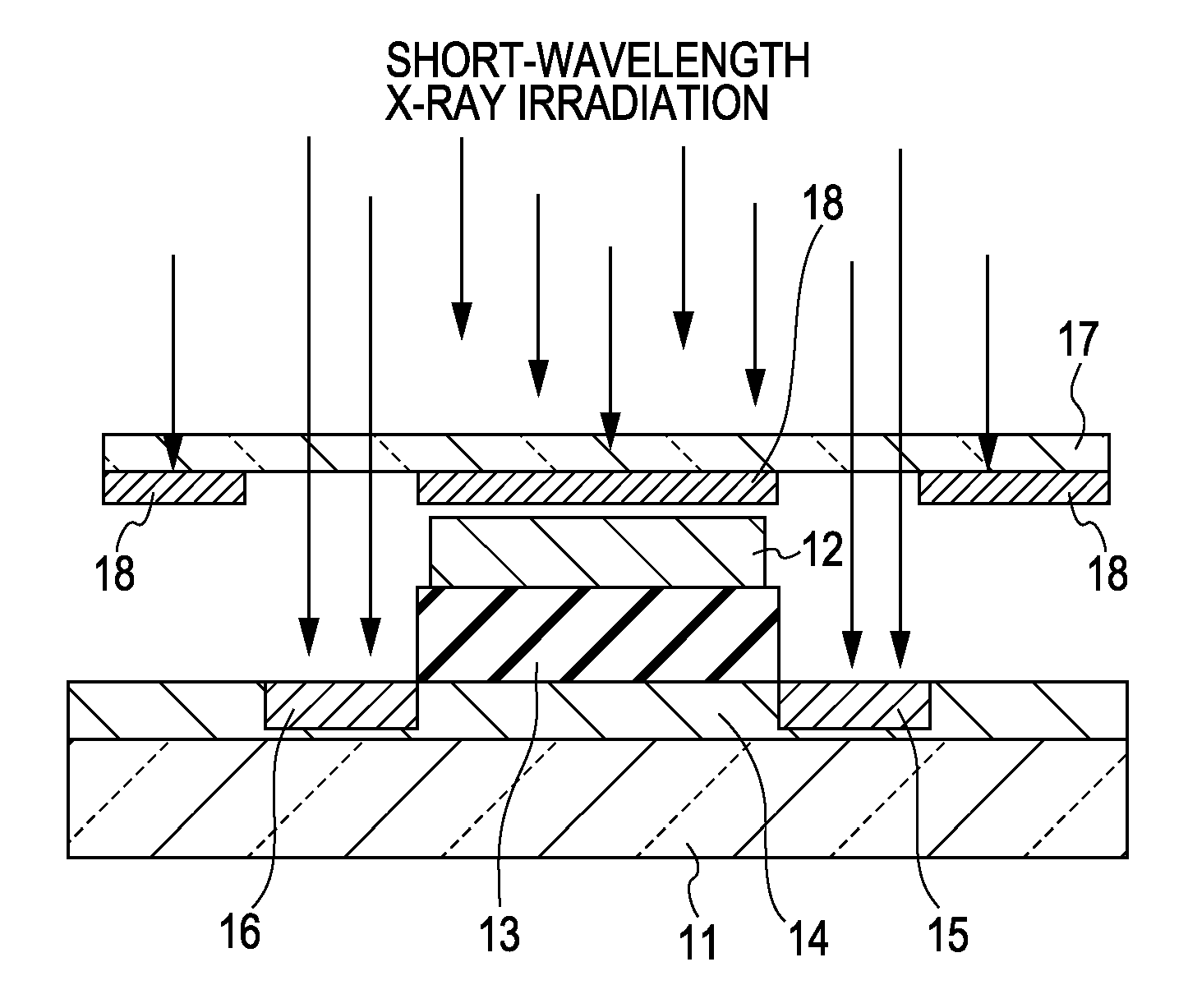
[0041] A method for fabricating an oxide-semiconductor device according to a First Embodiment of the present invention, specifically, a method for fabricating an FET using an oxide-semiconductor as a channel will now be described with reference to FIGS. 1 to 3. At first, the constitution of an FET device will be described with reference to the FET structure shown in FIG. 1.
[0042] In the FET shown in FIG. 1, an oxide semiconductor for the channel layer 14 may be formed of an oxide of which the primary constituent is ZnO, In2O3, or Ga2O3. In addition, the oxide semiconductor may be formed of an oxide mixture containing at least two of ZnO, In2O3, and Ga2O3 as the primary constituent. In particular, an oxide containing In2O3 and ZnO at a total molecular ratio of 50% or more is preferred. The present inventors have observed that these materials have excellent characteristics as an oxide semiconductor and of which conductivity is efficiently increased by irradiation with light or a part...
second embodiment
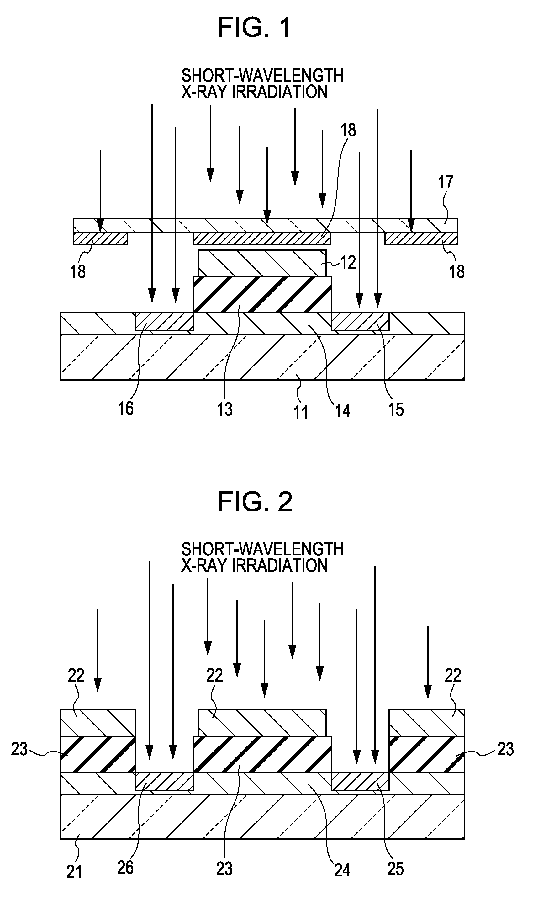
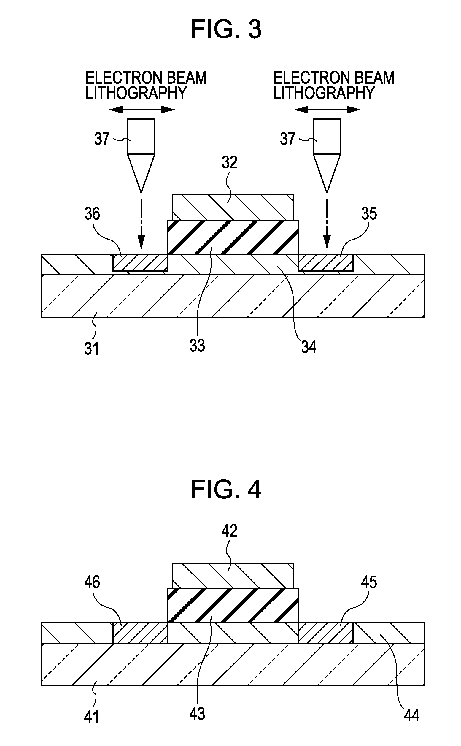
[0057] A method for fabricating an oxide-semiconductor device according to a Second Embodiment of the present invention, specifically, a method for fabricating an FET using an oxide-semiconductor as a channel will now be described with reference to FIGS. 4 to 7. At first, the constitution of an FET will be described with reference to the FET structure shown in FIG. 4.
[0058] In the FET device shown in FIG. 4, the oxide semiconductor for the channel layer 44 may be formed of an oxide of which the primary constituent is ZnO, In2O3, or Ga2O3. In addition, the oxide semiconductor may be formed of an oxide mixture containing at least two of ZnO, In2O3, and Ga2O3 as the primary constituent. In particular, an oxide containing In2O3 and ZnO at a total molecular ratio of 50% or more is preferred. The channel layer may contain an oxide semiconductor such as SnO2, TiOx, or another oxide semiconductor. In addition, the channel layer may be crystalline or amorphous.
[0059] When the desired devic...
example 1
[0067] A method for fabricating an FET of EXAMPLE 1 will now be described with reference to FIG. 1.
[0068] The FET fabricated in EXAMPLE 1 includes a substrate 11, a channel layer 14 disposed on the substrate 11, a gate-insulating film 13 on the channel layer 14, a gate electrode 12 on the gate-insulating film 13, a drain 15, and a source 16. The drain 15 and the source 16 are formed by increasing the conductivity of the channel layer 14 at both sides of the gate-insulating film 13. The substrate 11 is made of an insulative material. For example, a glass substrate can be used. In addition, an FET can be fabricated on a flexible substrate by using an organic material such as polyethylene terephthalate (PET) or a polymer material as the substrate 11.
[0069] Specifically, a film as a channel layer 14 is formed on a substrate 11 by sputtering an oxide semiconductor InGaZnO so as to have a film thickness of about 50 nm. The InGaZnO is amorphous and has a composition ratio In:Ga:Zn:O=1:1:...
PUM
 Abstract
Description
Claims
Application Information