Large-area magnetron sputtering chamber with individually controlled sputtering zones

a magnetron sputtering chamber and large-area technology, applied in vacuum evaporation coatings, electrolysis components, coatings, etc., can solve the problems of manufacturing difficulties, inability to create a large chamber, and inability to meet the requirements of advanced integrated circuits

Inactive Publication Date: 2007-03-15
APPLIED MATERIALS INC
View PDF87 Cites 318 Cited by
  • Summary
  • Abstract
  • Description
  • Claims
  • Application Information

AI Technical Summary

Benefits of technology

[0010] Embodiments of the invention may further provide a physical vapor deposition chamber assembly for depositing a layer on a large area substrate comprising: a target assembly comprising: one or more electrically insulating plates, two or more target sections that each have a first surface that is in contact with a processing region and a second surface that is in thermal contact with the one or more electrically insulating plates, and one or more gas ports that are in fluid communication with a gas source and the processing region, wherein at least one of the one or more gas ports is formed in at least one of the one or more electrically insulating plates, a plurality of power sources, each of the power sources coupled to at least one of the two or more target sections, and a substrate support positioned inside the physical vapor deposition processing chamber and having a substrate receiving surface, wherein a surface of a substrate positioned on the substrate receiving surface can be positioned to contact the processing region.
[0011] Embodiments of the invention may further provide a physical vapor deposition chamber assembly for depositing a layer on a large area substrate comprising: a target assembly comprising: one or more electrically insulating plates, and a first target section that has a first surface that is in contact with a processing region and a second surface that is in thermal contact with the one or more electrically insulating plates, wherein a first target section comprises a plurality of plates that are in electrical communication with each other, and a second target section that has a first surface that is in contact with a processing region and a second surface that is in thermal contact with the one or more electrically insulating plates, wherein a second target section comprises a plurality of plates that are in el

Problems solved by technology

However, conventional sputtering presents challenges in the formation of advanced integrated circuits on large area substrates, such a flat panel display substrates.
One issue that arises is that it is generally not feasible to create a chamber big enough to maintain the surface area ratio of the cathode (target) to anode surface area commonly used in conventional sputter processing chambers.
Trying to maintain the surfa

Method used


Image

  • Large-area magnetron sputtering chamber with individually controlled sputtering zones
  • Large-area magnetron sputtering chamber with individually controlled sputtering zones
  • Large-area magnetron sputtering chamber with individually controlled sputtering zones

Examples


Embodiment Construction

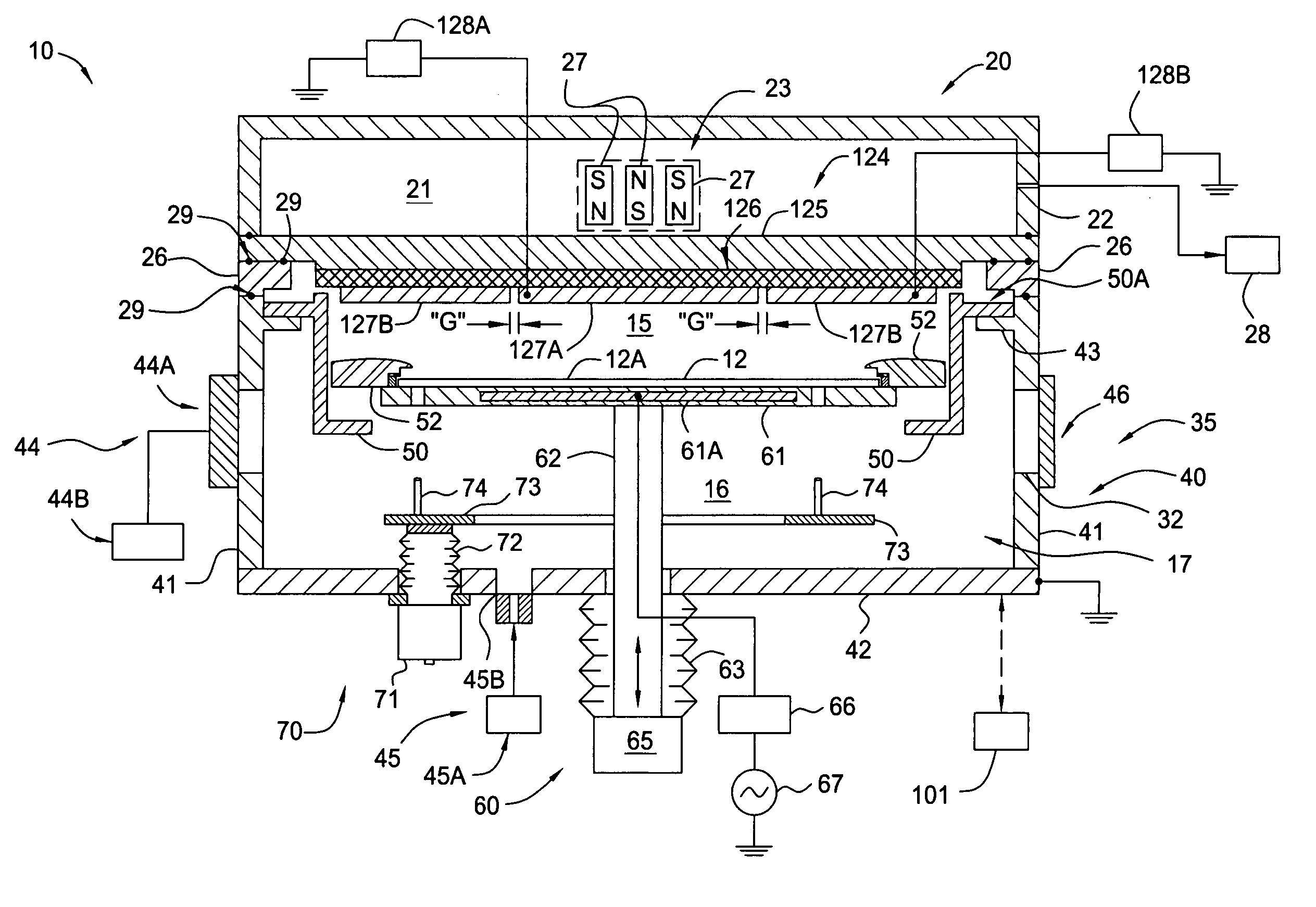
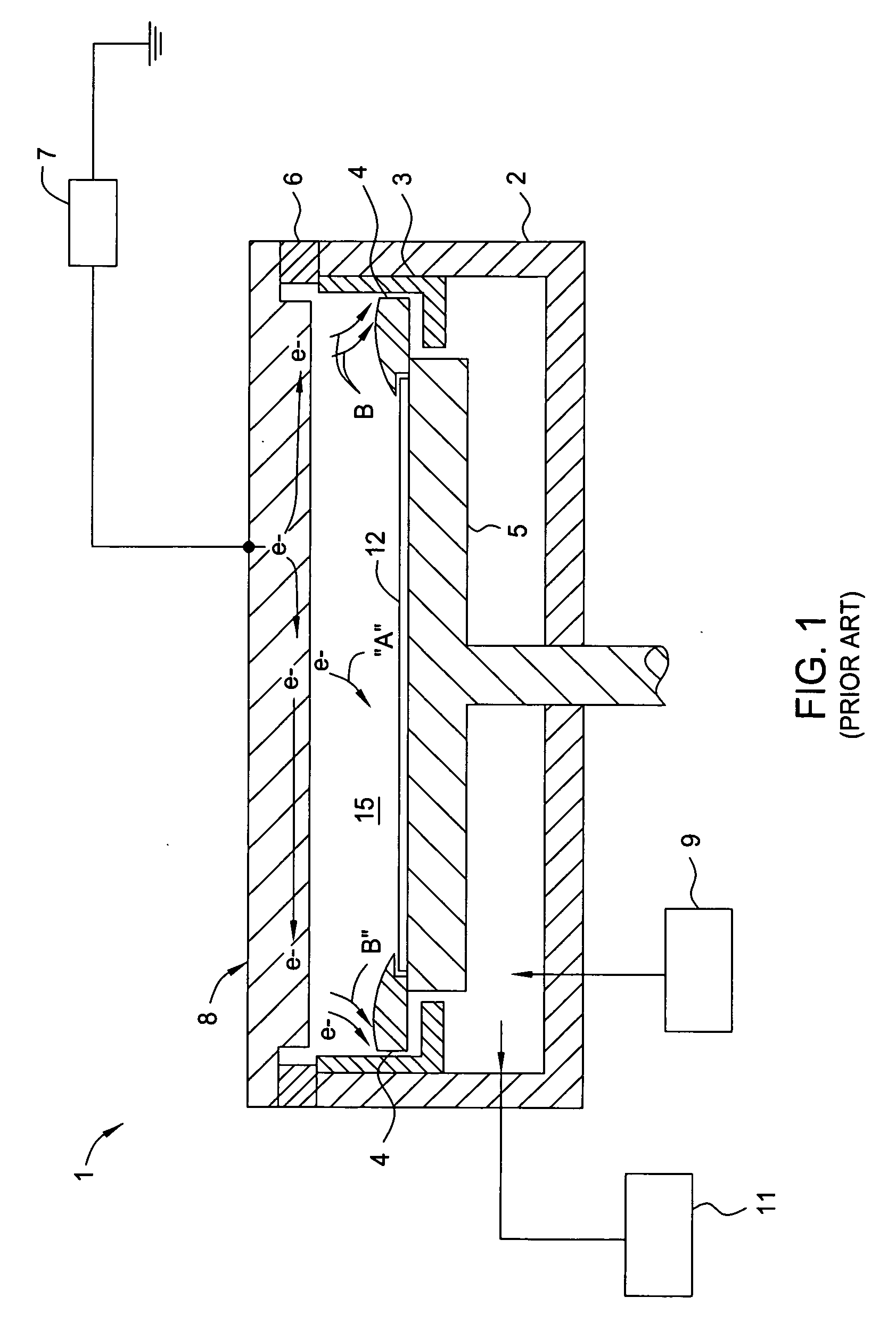
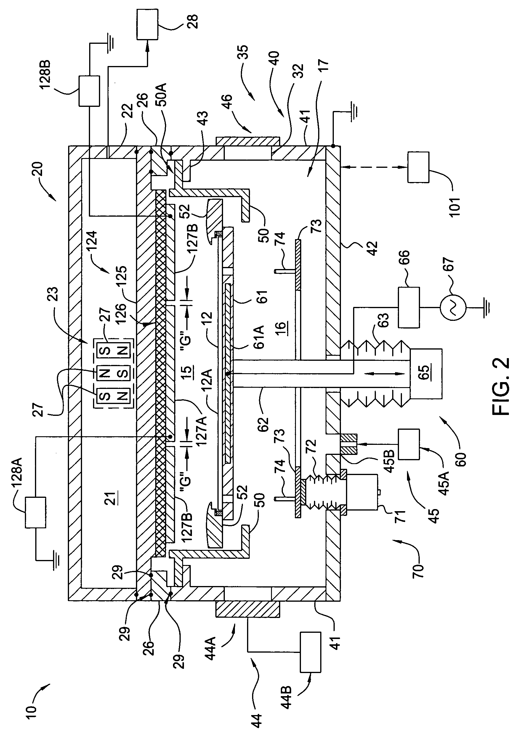
[0042] The present invention generally provides an apparatus and method for processing a surface of a substrate in a PVD chamber that has a sputtering target that has separately biasable sections, regions or zones to improve the deposition uniformity. In general, aspects of the present invention can be used for flat panel display processing, semiconductor processing, solar cell processing, or any other substrate processing. The invention is illustratively described below in reference to a physical vapor deposition system, for processing large area substrates, such as a PVD system, available from AKT, a division of Applied Materials, Inc., Santa Clara, Calif. In one embodiment, the processing chamber is adapted to process substrates that have a processing surface surface area of at least about 2000 cm2. In another embodiment, the processing chamber is adapted to process substrates that have a processing surface surface area of at least about 19,500 cm2 (e.g., 1300 mm×1500 mm). In ano...


PUM

PropertyMeasurementUnit
Areaaaaaaaaaaa
Magnetic fieldaaaaaaaaaa
Strengthaaaaaaaaaa

Abstract

The present invention generally provides an apparatus for processing a surface of a substrate in a physical vapor deposition (PVD) chamber that has a sputtering target that has separately biasable sections, regions or zones to improve the deposition uniformity. In general, aspects of the present invention can be used for flat panel display processing, semiconductor processing, solar cell processing, or any other substrate processing. In one aspect, each of the target sections of the multizone target assembly are biased at a different cathodic biases by use of one or more DC or RF power sources. In one aspect, each of the target sections of the multizone target assembly are biased at a different cathodic biases by use of one power source and one or more resistive, capacitive and/or inductive elements. In one aspect, the processing chamber contains a multizone target assembly that has one or more ports that are adapted deliver a processing gas to the processing region of the PVD chamber. In one aspect, the processing chamber contains a multizone target assembly that has one or more magnetron assemblies positioned adjacent to one or more of the target sections.

Description

BACKGROUND OF THE INVENTION [0001] 1. Field of the Invention [0002] Embodiments of the present invention generally relate to substrate plasma processing apparatuses and methods that are adapted to deposit a film on a surface of a substrate. [0003] 2. Description of the Related Art [0004] Physical vapor deposition (PVD) using a magnetron is one of the principal methods of depositing metal onto a semiconductor integrated circuit to form electrical connections and other structures in an integrated circuit device. During a PVD process a target is electrically biased so that ions generated in a process region can bombard the target surface with sufficient energy to dislodged atoms from the target. The process of biasing a target to cause the generation of a plasma that causes ions to bombard and remove atoms from the target surface is commonly called sputtering. The sputtered atoms travel generally toward the wafer being sputter coated, and the sputtered atoms are deposited on the wafer....

Claims


Application Information

Patent Timeline
IPC IPC(8): C23C14/00
CPCC23C14/3407C23C14/352
Inventor YE, YANWHITE, JOHNHOSOKAWA, AKIHIROLE, HIENMINH
Owner APPLIED MATERIALS INC
Why Eureka
Try Eureka