Process and system for etching doped silicon using SF6-based chemistry

a technology of sf6 and etching process, applied in process and machine control, sampled variable control system, instruments, etc., can solve the problem of limited etching effect of doped silicon layer

Inactive Publication Date: 2007-03-15
TOKYO ELECTRON LTD
View PDF12 Cites 12 Cited by
  • Summary
  • Abstract
  • Description
  • Claims
  • Application Information

AI Technical Summary

Problems solved by technology

However, as gate lengths are formed below 50 nm, FET scaling becomes limited by the

Method used


Image

  • Process and system for etching doped silicon using SF6-based chemistry
  • Process and system for etching doped silicon using SF6-based chemistry
  • Process and system for etching doped silicon using SF6-based chemistry

Examples


Embodiment Construction

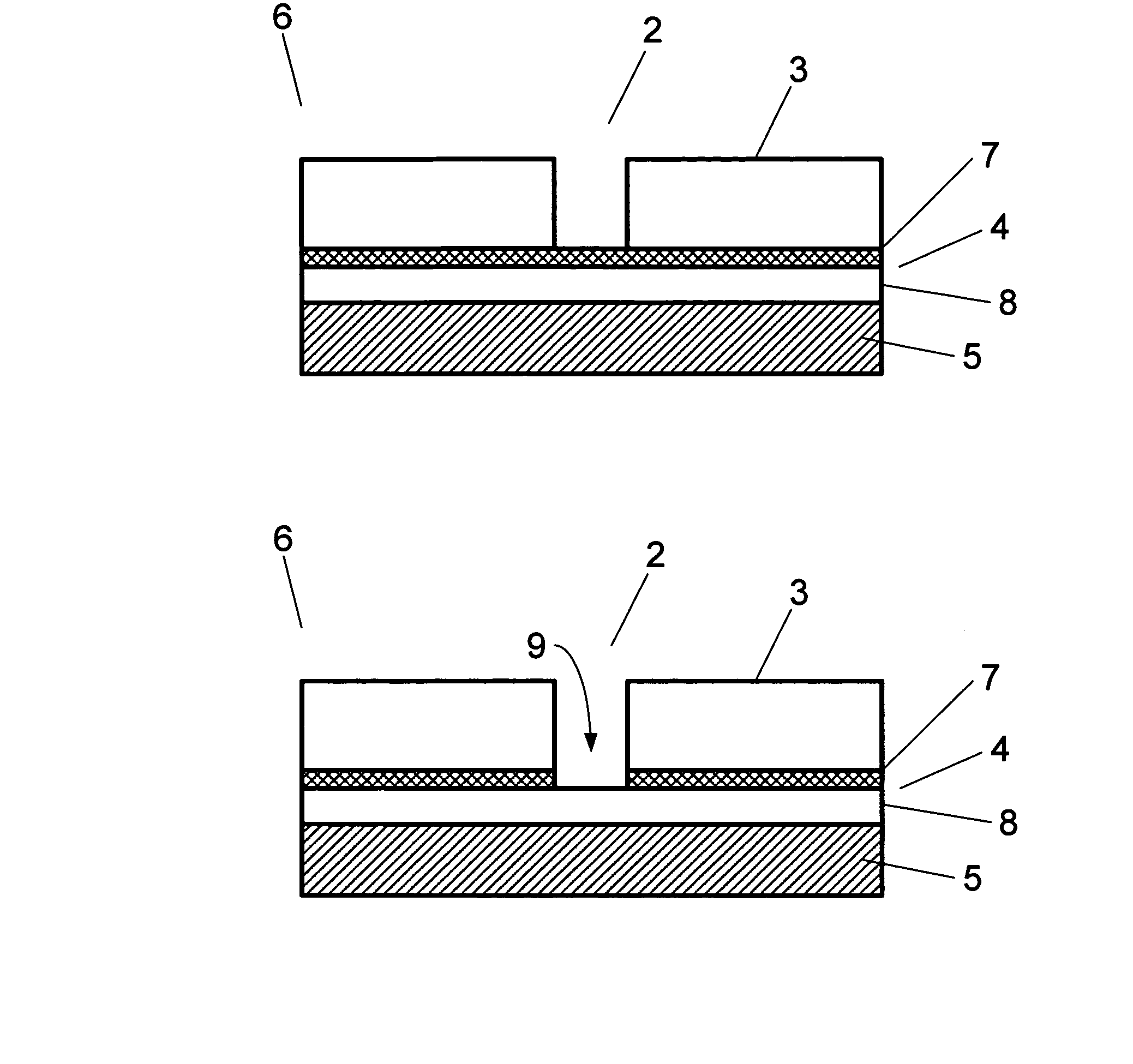
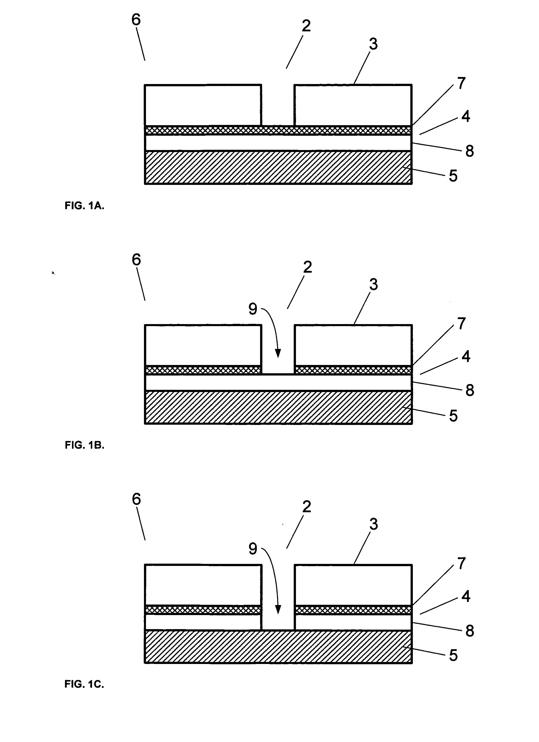
[0017] In material processing methodologies, pattern etching comprises the application of a thin layer of light-sensitive material, such as photoresist, to an upper surface of a substrate that is subsequently patterned in order to provide a mask for transferring this pattern to the underlying thin film during etching. The patterning of the light-sensitive material generally involves exposure by a radiation source through a reticle (and associated optics) of the light-sensitive material using, for example, a micro-lithography system, followed by the removal of the irradiated regions of the light-sensitive material (as in the case of positive photoresist), or non-irradiated regions (as in the case of negative resist) using a developing solvent.

[0018] For example, as shown in FIGS. 1A-C, an etching mask 6 comprising light-sensitive layer 3 with pattern 2 formed using conventional lithographic techniques can be utilized as a mask for etching a silicon layer 4, wherein the mask pattern ...


PUM

PropertyMeasurementUnit
Fractionaaaaaaaaaa
Etch rateaaaaaaaaaa
Etch rateaaaaaaaaaa

Abstract

A process and system for anisoptropically dry etching through a doped silicon layer is described. The process chemistry comprises SF6 and a fluorocarbon gas. For example, the fluorocarbon gas can include CxFy, where x and y are integers greater than or equal to unity, for example, C4F8.

Description

CROSS-REFERENCE TO RELATED APPLICATIONS [0001] This application is related to co-pending U.S. application Ser. No. 11 / ______, entitled “Process and System For Etching Doped Silicon”, attorney reference 313530-P0019, filed on even date herewith. The entire contents of this application is herein incorporated by reference in its entirety.FIELD OF THE INVENTION [0002] The present invention relates to a method and system for etching a doped silicon layer on a substrate using a dry plasma process, and more particularly to a method and system for etching a doped silicon layer using a process gas comprising SF6 and a fluorocarbon gas. BACKGROUND OF THE INVENTION [0003] As is known to those in the semiconductor art, the reduction in size of semiconductor devices has been indispensably necessary in order to cause an increase in device performance and a decrease in power consumption. For instance, in keeping with the pace of modern technology, integrated circuits (ICs), including, for example,...

Claims


Application Information

Patent Timeline
IPC IPC(8): C23F1/00G05B21/00H01L21/302H01L21/306
CPCH01L21/32137H01L21/67069H01L2924/0002H01L2924/00H01L21/3065
Inventor KO, AKITERU
Owner TOKYO ELECTRON LTD
Why Eureka
Try Eureka