Lithographic apparatus and device manufacturing method

a technology of lithographic equipment and manufacturing method, which is applied in the direction of printers, radiation therapy, therapy, etc., can solve the problem that the output power of euv lithography sources cannot be changed, and achieve the effect of high measurement accuracy

Active Publication Date: 2007-03-15
ASML NETHERLANDS BV
View PDF4 Cites 4 Cited by
  • Summary
  • Abstract
  • Description
  • Claims
  • Application Information

AI Technical Summary

Benefits of technology

[0010] One aspect of embodiments of the present invention to provide novel lithographic apparatus enabling high measurement accuracy in the control of the intensity of the projection beam incident on the substrate.
[0012] Thus the attenuation control device, which is typically in the form of a series of venetian blinds (the ‘blades’), can be used to correct for non-uniformity to a high level of accuracy, and to decrease the overall intensity of the beam. This is useful because, as previously indicated, EUV lithography sources are not capable of changing their output power. Because a single source is used to supply detecting radiation to all of the position detectors, the number of components is decreased, resulting in lower cost, more space, greater reliability and less heat generation coupled with better possibilities for cooling. Also inaccuracies due to fluctuations or temperature variations are largely avoided, and the mechanical adjustment of the arrangement becomes more straightforward.

Problems solved by technology

This is useful because, as previously indicated, EUV lithography sources are not capable of changing their output power.

Method used


Image

  • Lithographic apparatus and device manufacturing method
  • Lithographic apparatus and device manufacturing method
  • Lithographic apparatus and device manufacturing method

Examples


Embodiment Construction

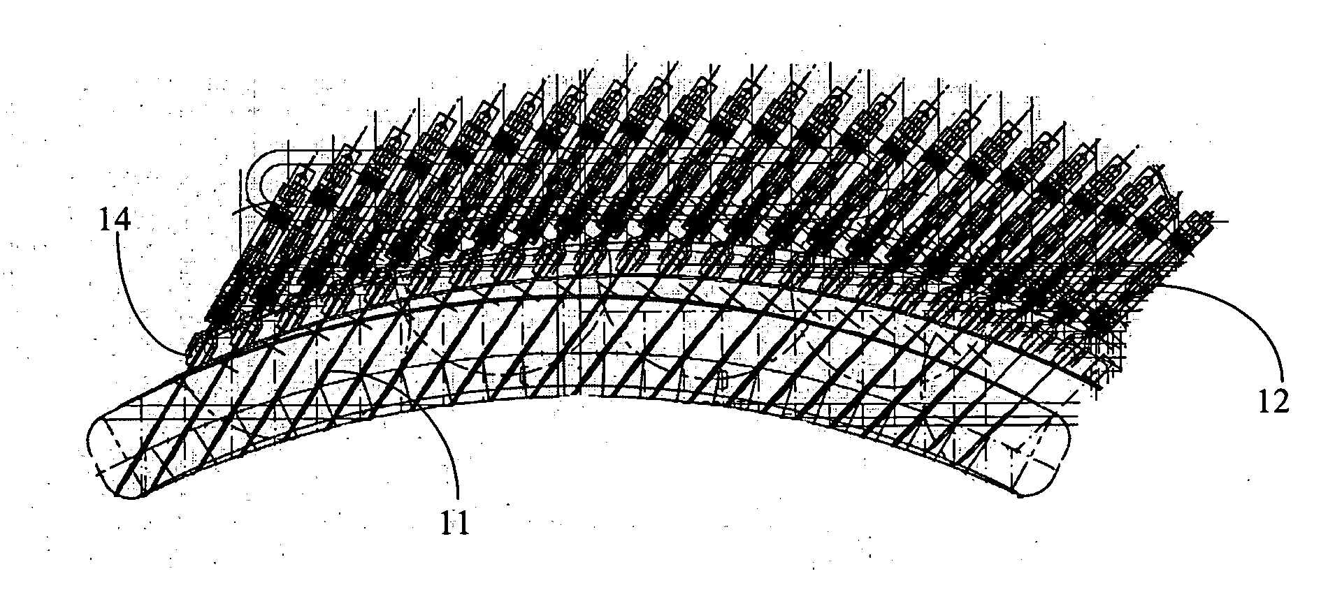
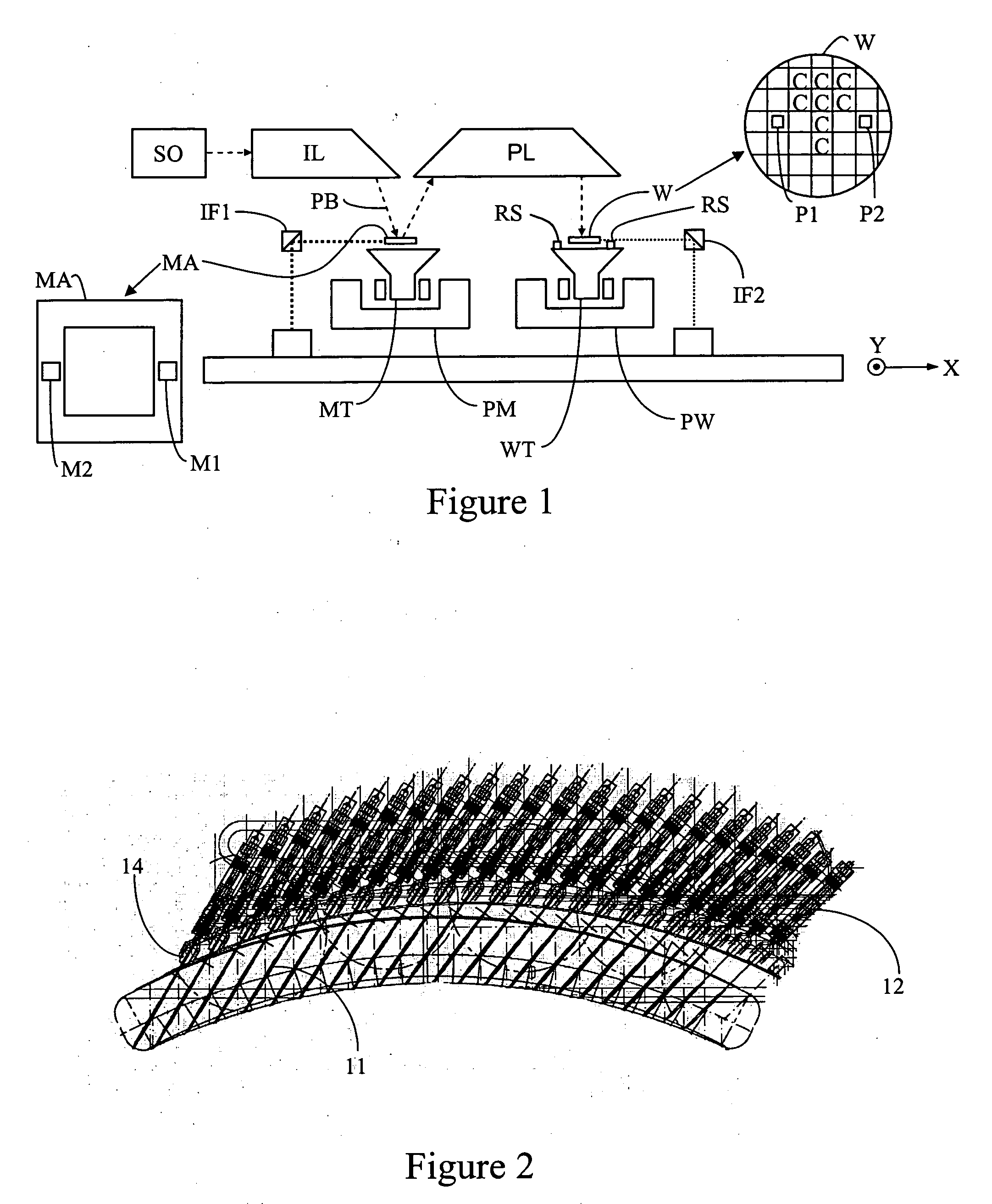
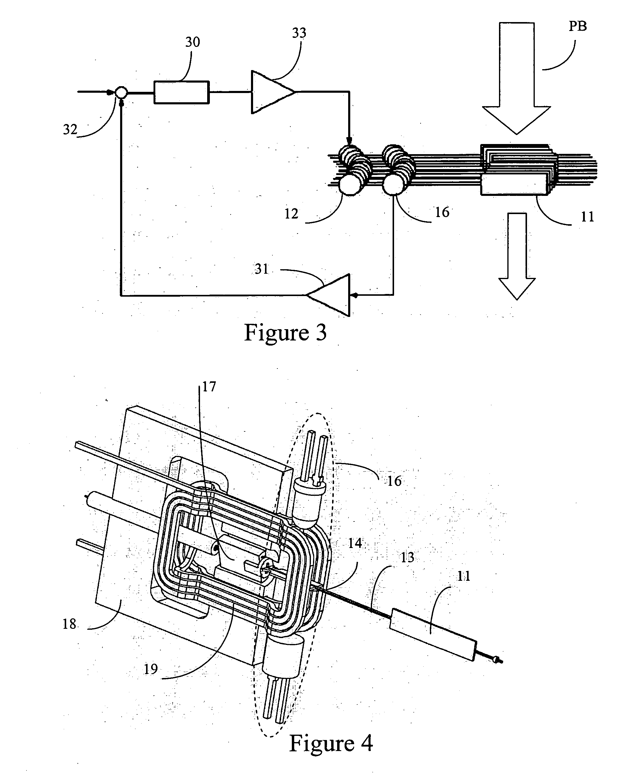
[0042]FIG. 1 schematically depict an example of a lithographic apparatus. The apparatus includes: [0043] an illumination system (illuminator) IL for providing a projection beam PB of radiation (e.g. UV radiation). [0044] a support structure (e.g. a mask table) MT for supporting patterning means (e.g. a mask) MA and connected to first positioning means PM for accurately positioning the patterning means with respect to item PL; [0045] a substrate table (e.g. a wafer table) WT for holding a substrate (e.g. a resist-coated wafer) W and connected to second positioning means PW for accurately positioning the substrate with respect to item PL; and [0046] a projection system (e.g. a refractive or reflective projection lens) PL for imaging a pattern imparted to the projection beam PB by patterning means MA onto a target portion C (e.g. comprising one or more dies) of the substrate W.

[0047] The illumination system may include various types of optical components, such as refractive, reflectiv...


PUM

PropertyMeasurementUnit
fixed angleaaaaaaaaaa
wavelengthaaaaaaaaaa

Abstract

An attenuation adjustment device is disposed in a radiation system of a lithography device and includes a plurality of members for casting penumbras in the radiation beam illuminating the patterning device. Furthermore an attenuation control device is provided for adjusting the members in such a manner as to control the attenuation of the patterned radiation beam projected onto the target portion of the substrate across the cross-section of the patterned radiation beam. The attenuation control device incorporates a detector for providing an output indicative of the position of each member in dependence on detection of a beam of detecting radiation reaching the angle detector after attenuation by the member.

Description

FIELD OF THE INVENTION [0001] The present invention relates to a lithographic apparatus and a device manufacturing method. BACKGROUND TO THE INVENTION [0002] A lithographic apparatus is a machine that applies a desired pattern onto a target portion of a substrate. Lithographic apparatus can be used, for example, in the manufacture of integrated circuits (ICs). In that instance, a patterning device, which is alternatively referred to as a mask or a reticle, may be used to generate a circuit pattern corresponding to an individual layer of the IC, and this pattern can be imaged onto a target portion (e.g. comprising part of, one or several dies) of a substrate (e.g. a silicon wafer) that has a layer of radiation-sensitive material (resist). In general, a single substrate will contain a network of adjacent target portions that are successively exposed. Lithographic apparatus may be of the transmissive type, where radiation is passed through a mask to generate the pattern, or of the refl...

Claims


Application Information

Patent Timeline
Patent Type & Authority Applications(United States)
IPC IPC(8): G03F7/20
CPCG03F7/70191G03F7/70083
Inventor NEERHOF, HENDRIK ANTONY JOHANNESBOTMA, HAKORAVENSBERGEN, MARIUS
Owner ASML NETHERLANDS BV
Why Eureka
Try Eureka