

Solid state imaging device, method of producing the same and camera relating to same
- Summary
- Abstract
- Description
- Claims
- Application Information
AI Technical Summary
Benefits of technology
Problems solved by technology
Method used
Image

Examples
first embodiment
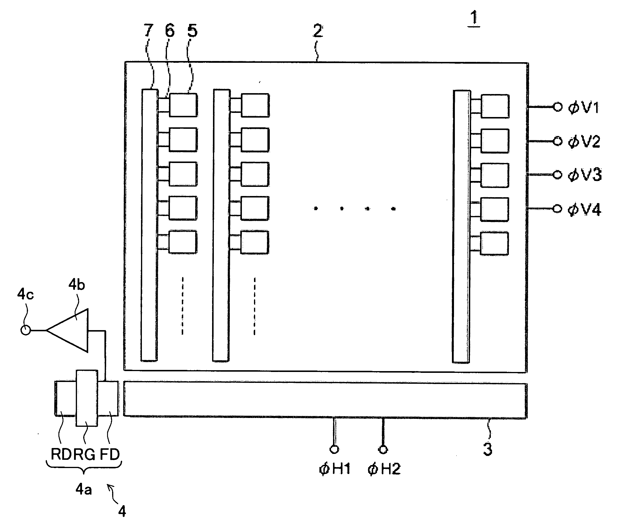
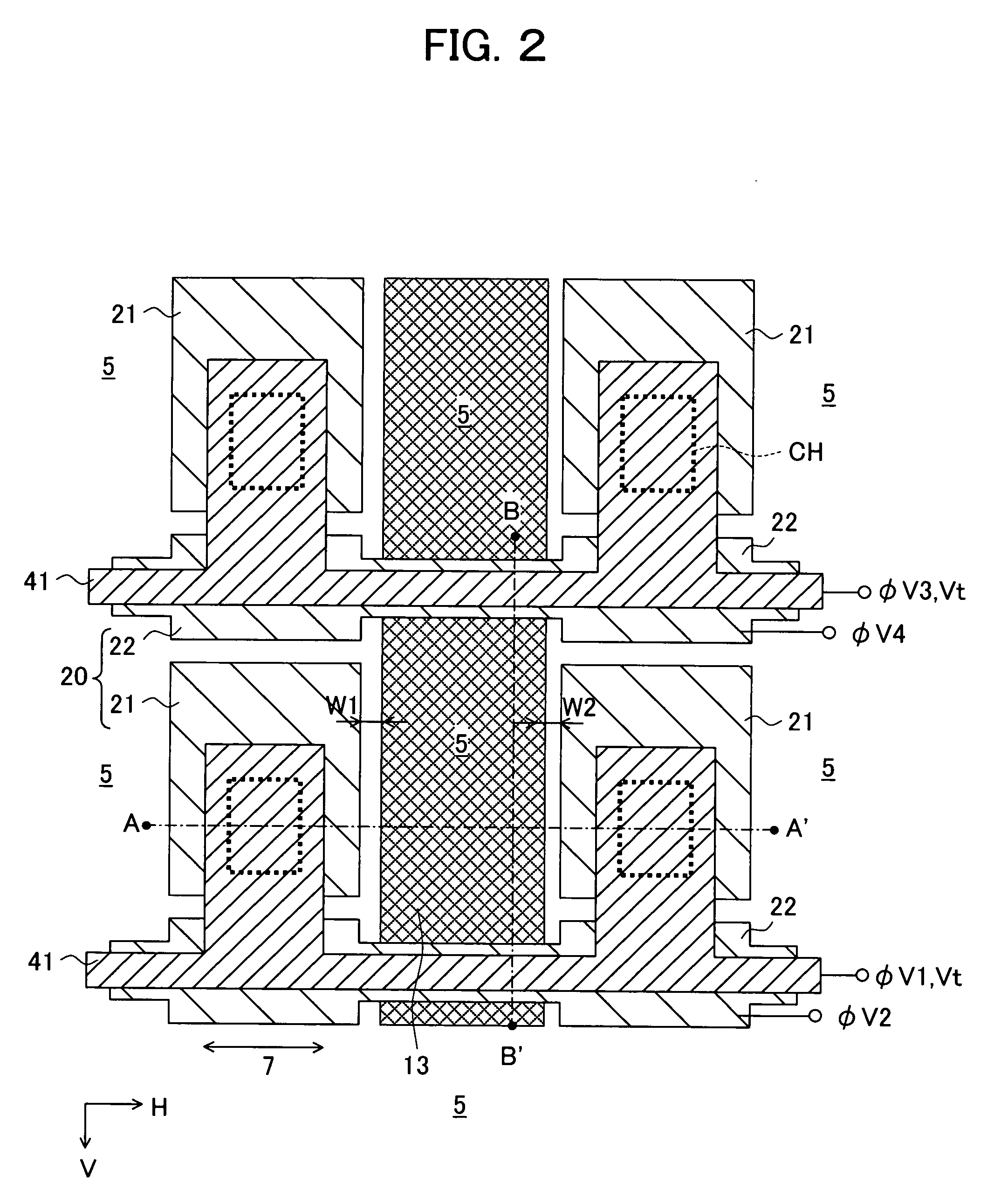
[0071] The transfer electrodes 20 have single-layer structures, for example, are formed by single layers of polycrystalline silicon. In the first embodiment, two transfer electrodes are arranged for each light receiving portion 5.
[0072] A first transfer electrode 21 is arranged adjacent to each light receiving portion 5 in the horizontal direction. The first transfer electrodes 21 arranged corresponding to the different light receiving portions 5 are arranged isolated in the horizontal and vertical directions.
[0073] A second transfer electrode 22 is arranged while passing between the light receiving portions 5 adjacent in the vertical direction and extending in the horizontal direction. In each vertical transfer portion 7, the first transfer electrodes 21 and the second transfer electrodes 22 are alternately arranged.
[0074] Each first drive interconnect 41 extending in the horizontal direction is arranged so as to overlap the second transfer electrode 22 extending in the horizonta...
second embodiment
[0145] On each transfer channel 14, a first transfer electrode 121, a third transfer electrode 123, and a second transfer electrode 122 are repeatedly arranged in the transfer direction in a state where the insulation films are interposed. The first transfer electrode 121, the second transfer electrode 122, and the third transfer electrode 123, may be simply referred to as the “transfer electrodes 120”. The vertical transfer portions 7 are formed by the transfer channels 14 and the transfer electrodes 120. The transfer electrodes 120 have single-layer structures, for example, are formed by single layers of polycrystalline silicon. In the second embodiment, three transfer electrodes are arranged for each light receiving portion 5.
[0146] The first transfer electrode 121 is formed so as to extend in the horizontal direction while passing between light receiving portions 5 adjacent in the vertical direction. The first transfer electrodes 121 are arranged crossing the transfer channel 14...
PUM
 Abstract
Description
Claims
Application Information