Integrated circuit with dynamic memory allocation

Active Publication Date: 2007-03-22
III HLDG 6
View PDF1 Cites 16 Cited by
  • Summary
  • Abstract
  • Description
  • Claims
  • Application Information

AI Technical Summary

Benefits of technology

[0011] Accordingly, by using the local memory LM, whenever possible, before data is outsourced to the global memory GM, power as well as bandwidth of the interconnect means can be saved. Furthermore, sufficient flexibility is introduced to the system on-chip to enable running applications that dem

Problems solved by technology

On the other hand, with the above described trend of convergence of many consumer electronics markets like mobile phones, PDAs, MP

Method used


Image

  • Integrated circuit with dynamic memory allocation
  • Integrated circuit with dynamic memory allocation

Examples


Example

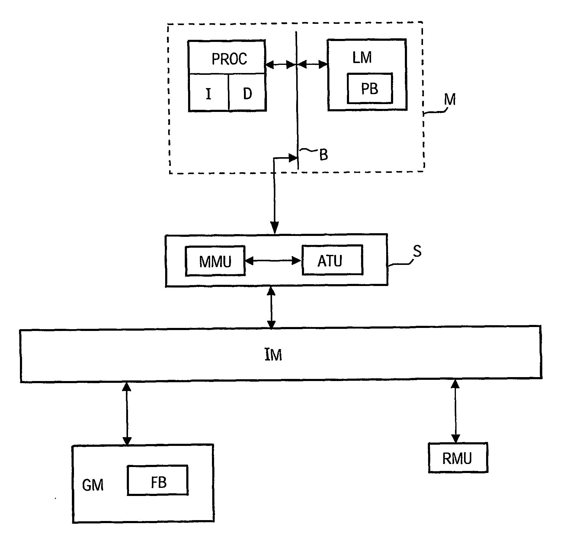
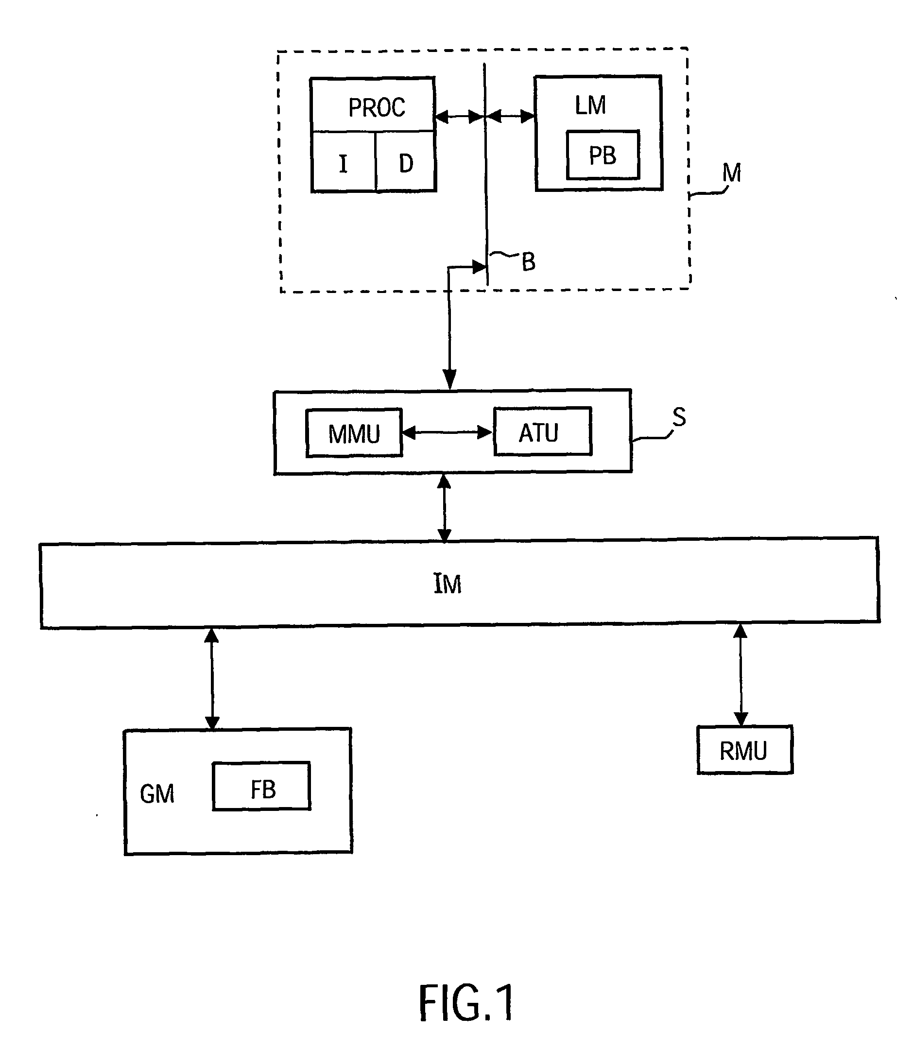
[0023]FIG. 1 shows a block diagram of a system or chip according to a first embodiment. The system comprises a module M, a shell S, an interconnect means IM, a global memory GM and a resource managing unit RMU. The module M is connected to the global memory GM via the shell S and the interconnect means IM. The module M comprises a processor PROC, an instruction cache I, a data cache D, and a local memory LM. The processor PROC and the local memory LM are connected to each other via a bus B. The local memory LM comprises a prefetch buffer PB. The local memory LM is used as a private memory exclusively for the module M. The local memory LM is dimensioned as a small memory which is enough to run applications with low memory demands. The amount of this memory space may depend on the application performed on the module M.

[0024] The module M may be any subsystem and may further comprise other functional blocks, performing dedicated applications or several different applications. Although...

Example

[0032] According to a second embodiment of the invention, the module M from FIG. 1 may be an UMTS modem, which requires memory to perform a de-interleaving function. The amount of required memory for this function will depend on the data rate, the interleaving span (the amount of ms interleaving) and the coding rate of the error correction. If the memory is dimensioned for the maximum data rate and the maximum span, a memory of 2 Mbits is required. Usually, such a large amount of data have to be located in the global memory GM. On the other hand, if a low-demanding case at low data rate and minimum interleaving span is considered, merely 50kbits are required. This amount of memory space can easily be stored in the local memory LM, therefore, this will lead to a power advantage, since no data needs to be outsourced. Thus, reducing the power needed by a mobile phone is always preferable, since this is a prime competing factor (“talk-time”) of a mobile phone.

[0033] It should be noted ...


PUM


Abstract

An integrated circuit comprising a plurality of modules (M) for processing applications is provided, wherein each of said modules comprise a local memory (LM). The integrated circuit further comprises a global memory (GM), which can be shared between the plurality of modules (M), and an interconnect means (IM) for interconnecting said modules (M) and said global memory (GM). A memory managing unit (MMU) is associated to each of said modules (M) and determines whether the local memory (LM) provides sufficient memory space for the currently processed application. If this is not the case, the memory managing unit (MMU) requests a global buffer (FB) in said global memory (GM) to be exclusively reserved for the processing data of its associated module (M). Accordingly, by using the local memory (LM), whenever possible, before data is outsourced to the global memory (GM), power as well as bandwidth of the interconnect means can be saved. Furthermore, sufficient flexibility is introduced to the system on-chip to enable running applications that demand more local resources e.g. local memory, than are available in the subsystems or modules (M), without having the need to design the subsystems or modules for worst case scenarios. Especially, when the worst-case demands are much higher than the average case, the cost advantage can be significant.

Description

FIELD OF THE INVENTION [0001] The invention relates to an integrated circuit comprising a plurality of modules and a method for memory allocation in such an integrated circuit. BACKGROUND OF THE INVENTION [0002] With the recent development of computation and communication resources two main trends in the architecture of mobile terminals have risen. The first trend is the application convergence and increasing diversity, e.g. more and more diverse functions or subsystems are integrated into a single terminal enabling the terminal to perform new services and applications. The second trend is directed to the aggravation of architecture complexity, e.g. the overall complexity of both hardware and software architectures exceeds the limits of conventional architectures style based on cores connected by buses. [0003] One possible solution to meet for the above mentioned trends appears to be modularity. When the boundaries of modules are chosen to coincide with functional subsystems like GS...

Claims


Application Information

Patent Timeline
IPC IPC(8): G11C7/10G06F12/02G06F12/08G06F12/084G06F12/0842G06F12/0862
CPCG06F12/084Y02B60/1225G06F12/0862G06F12/0842Y02D10/00
Inventor HARMSZE, FRANCOISE JEANNETTEBURCHARD, ARTUR TADEUSZKENTER, HARMS JAN HILTJO NANNO
Owner III HLDG 6
Why Eureka
Try Eureka