
Polysilicon thin film fabrication method
a thin film and polysilicon technology, applied in the direction of basic electric elements, electrical equipment, semiconductor devices, etc., can solve the problems of non-uniform characteristics, inability to achieve uniform grain size, and inability to accurately control the growth of grain in two or three dimensions, so as to improve the electrical characteristics of tfts, improve the uniformity of device parts of the drive circuit, and control stably
- Summary
- Abstract
- Description
- Claims
- Application Information
AI Technical Summary
Benefits of technology
Problems solved by technology
Method used
Image

Examples
Embodiment Construction
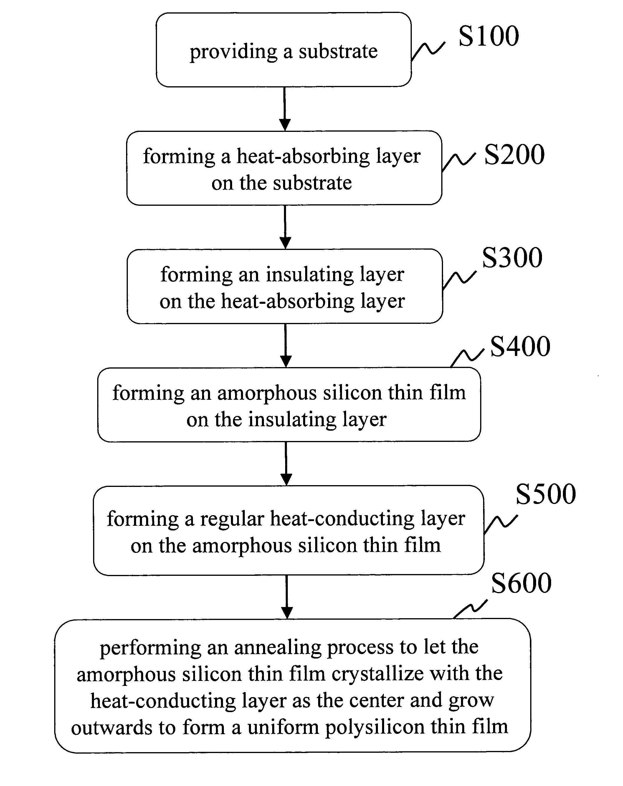
[0020] As shown in FIG. 4, the present invention provides a polysilicon thin film fabrication method, which comprises the following steps.
[0021] First, a substrate is provided (Step S100). The substrate is a glass substrate, an insulator substrate, or a semiconductor substrate. Next, a heat-absorbing layer is formed on the substrate (Step S200). An insulating layer is then formed on the heat-absorbing layer (Step S300). Subsequently, an amorphous silicon thin film is formed on the insulating layer (Step S400). A regular heat-conducting layer is formed on the amorphous silicon thin film (Step S500). Finally, An annealing process is performed to let the amorphous silicon thin film crystallize with the heat-conducting layer as the center and grow outwards to form a uniform polysilicon thin film.
[0022] The present invention will be exemplified below with reference to FIGS. 5A-5H and FIGS. 6A-6C. The polysilicon thin film fabrication method of the present invention comprises the follow...
PUM
| Property | Measurement | Unit |
|---|---|---|
| thickness | aaaaa | aaaaa |
| thickness | aaaaa | aaaaa |
| reflectivity | aaaaa | aaaaa |
Abstract
Description
Claims
Application Information