Semiconductor device and manufacturing method thereof

Inactive Publication Date: 2007-03-22
KK TOSHIBA
View PDF5 Cites 27 Cited by
  • Summary
  • Abstract
  • Description
  • Claims
  • Application Information

AI Technical Summary

Benefits of technology

[0013] According to another aspect of the present invention, it is provided a semiconductor device comprising: a first switching element device whose electrical conductivity is governed by a first carrier; a first conductive stress applying layer to apply a first stress to enhance mobility of the first carrier in the first switching element device; a second swi

Problems solved by technology

However, a sufficient improvement in the current driving force cannot be expected by a simple reduction in the gate length with progress of miniaturization in recent years.
However, in the pMOS, since a carrier flowing through the channel is a hole, and thus its mobility reduces.
Accordingly, there arises a problem that a driving current is decreased in the pMOS.
Therefore, if only one kind of silicide is used, a current driving force of one of the nMOS and the pMOS can be improved, but a current driving force of the remaining one is disad

Method used


Image

  • Semiconductor device and manufacturing method thereof
  • Semiconductor device and manufacturing method thereof
  • Semiconductor device and manufacturing method thereof

Examples


Embodiment Construction

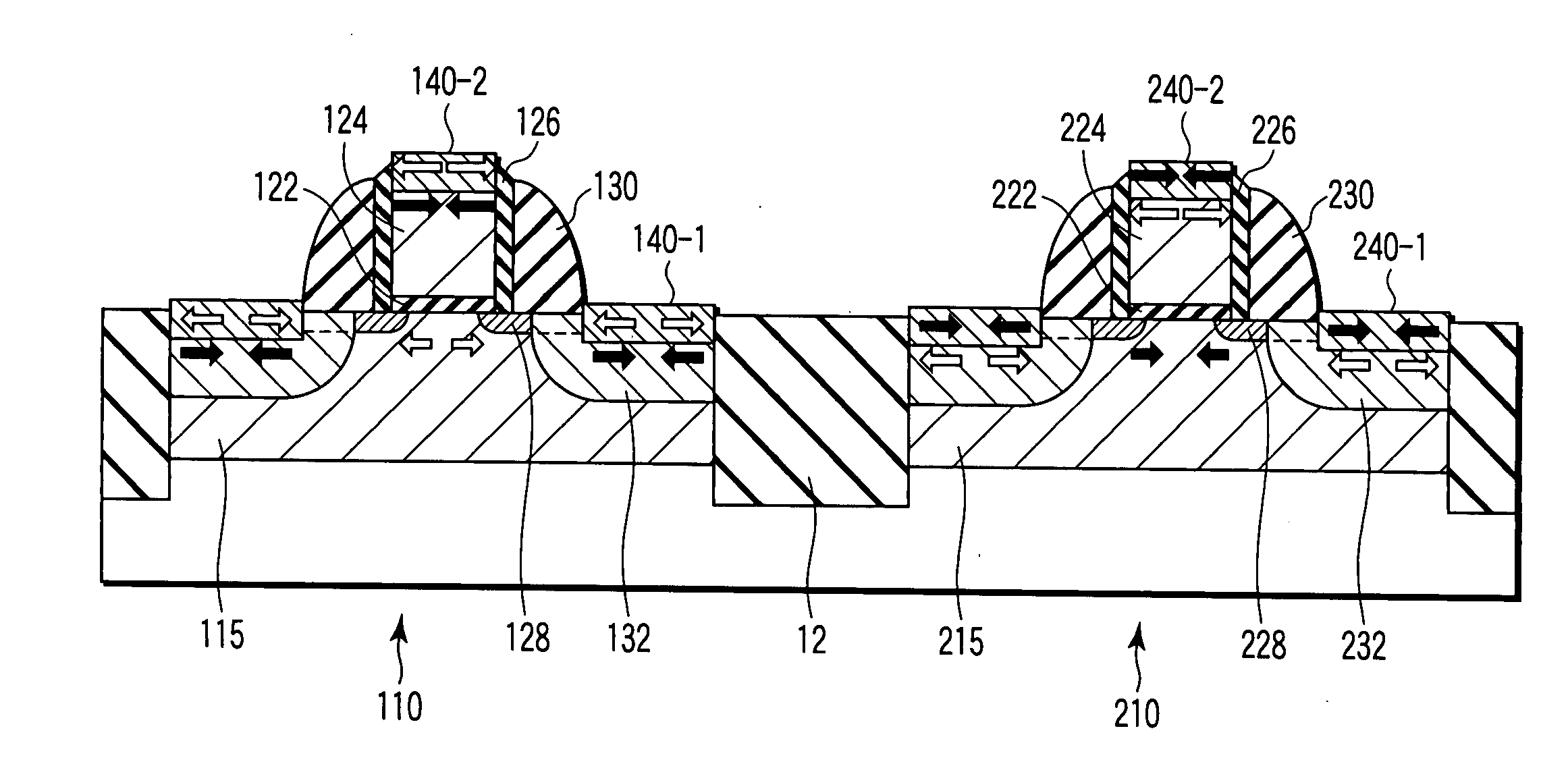
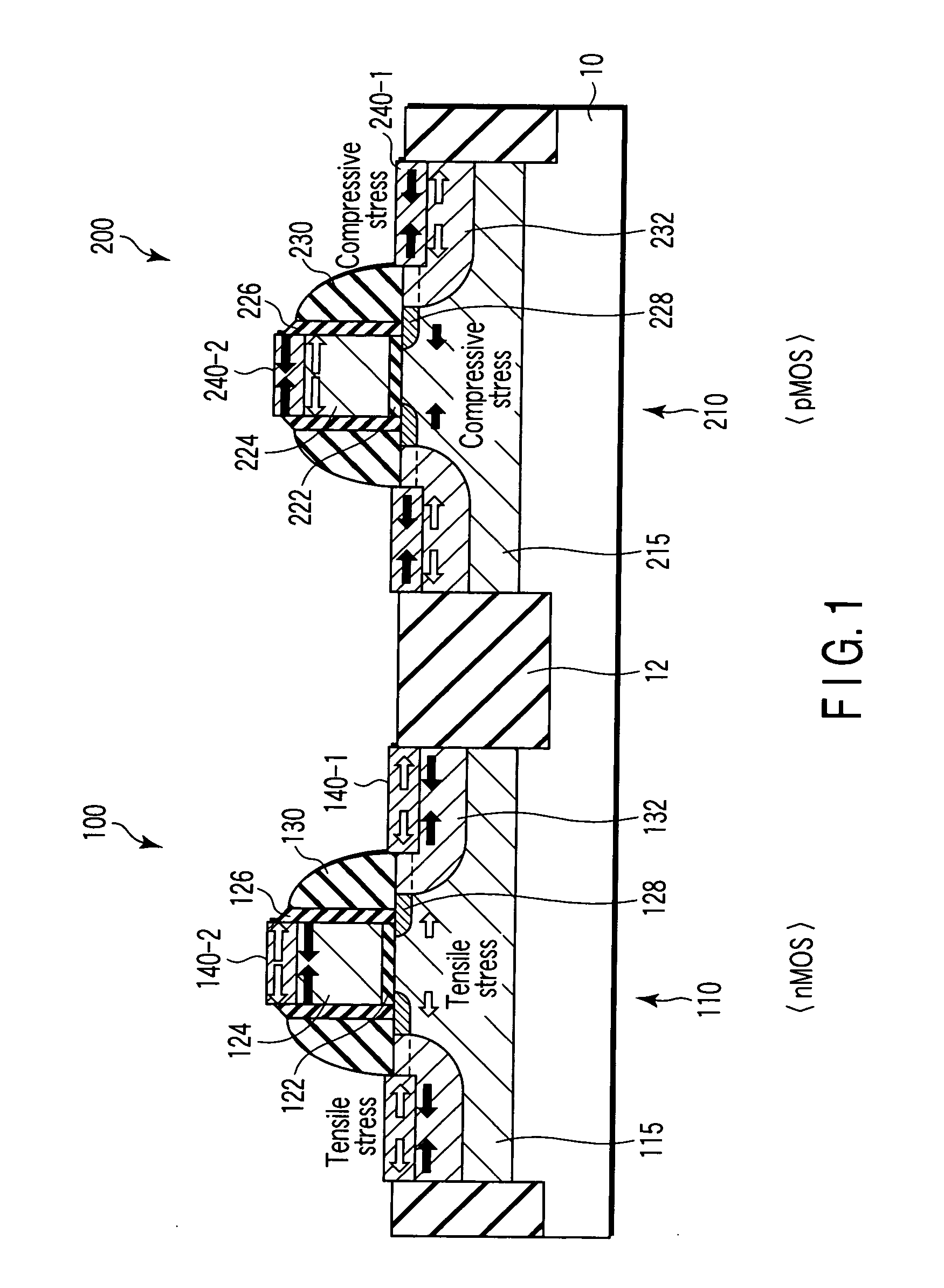
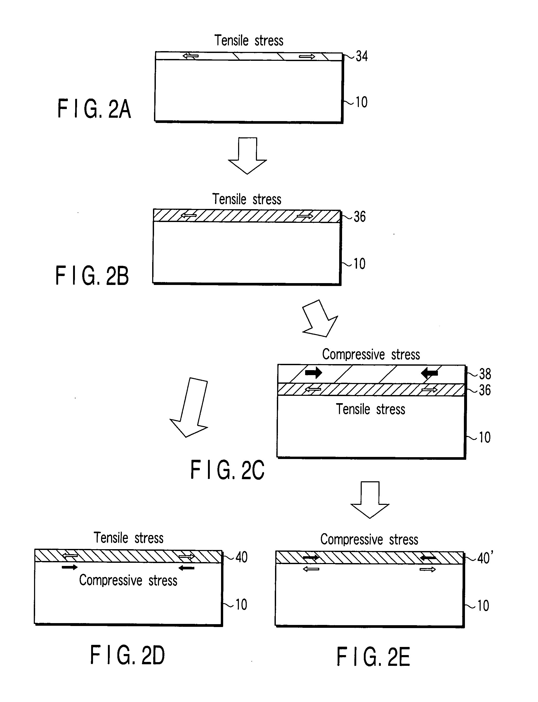
[0018] The embodiments of the present invention will be described with reference to the accompanying drawings. Throughout the drawings, corresponding portions are denoted by corresponding reference numerals. Each of the following embodiments is illustrated as one example, and therefore the present invention can be variously modified and implemented without departing from the spirits of the present invention.

[0019] The present invention discloses a semiconductor device and a manufacturing method thereof which can improve characteristics of each of an nMOS and a pMOS even though miniaturization is effected.

[0020] According to the present invention, it is provided a semiconductor device comprising a silicide layer which gives a tensile stress to a channel region of the nMOS and another silicide layer which gives a compressive stress to a channel region of the pMOS, and a manufacturing method thereof. The silicide layers are of one kind of silicide constituted of the same element, and...


PUM


Abstract

The present invention discloses a semiconductor device and a manufacturing method thereof which improves its characteristics even though it is miniaturized. According to one aspect of the present invention, it is provided a semiconductor device comprising a first semiconductor element device including a pair of first diffusion layers formed in the semiconductor substrate with a first gate electrode therebetween, and a first conductor layer formed in the first diffusion layer and having an internal stress in a first direction, and a second semiconductor element device including a pair of second diffusion layers formed in the semiconductor substrate with a second gate electrode therebetween, and a second conductor layer formed in the second diffusion layer, having an internal stress in a second direction opposite to the first direction, and constituted of the same element as that of the first conductor layer.

Description

CROSS-REFERENCE TO RELATED APPLICATIONS [0001] This application is based upon and claims the benefit of priority from prior Japanese Patent Application No. 2005-270773, filed Sep. 16, 2005, the entire contents of which are incorporated herein by reference. BACKGROUND OF THE INVENTION [0002] 1. Field of the Invention [0003] The present invention relates to a semiconductor device and a manufacturing method thereof, and more particularly to a semiconductor device using a silicide and a manufacturing method thereof. [0004] 2. Description of the Related Art [0005] In a recent miniaturized semiconductor device, especially in a metal insulator semiconductor (MIS) type field effect transistor (FET) device, it has been demanded to improve characteristics of the semiconductor device, such as an increase in a speed and a reduction in power consumption. In order to increase the speed of the semiconductor device, it is required to improve a current driving force of an active component. In a conv...

Claims


Application Information

Patent Timeline
IPC IPC(8): H01L21/8238
CPCH01L21/823807H01L29/7845H01L21/823814H01L29/7833H01L29/6659
Inventor IINUMA, TOSHIHIKO
Owner KK TOSHIBA
Why Eureka
Try Eureka