
Gallium nitride based semiconductor light emitting diode and method of manufacturing the same

a technology of light-emitting diodes and gallium nitride, which is applied in the direction of semiconductor devices, basic electric elements, electrical appliances, etc., can solve the problems of more serious problems, b>100/b> is not quickly dissipated, and heat generation, so as to improve the heat dissipation capability of sapphire substrates, improve the luminous efficiency of devices, and improve the effect of heat dissipation capability

Inactive Publication Date: 2007-03-29
SAMSUNG ELECTRO MECHANICS CO LTD
View PDF2 Cites 50 Cited by
  • Summary
  • Abstract
  • Description
  • Claims
  • Application Information

AI Technical Summary

Benefits of technology

The present invention provides a GaN based semiconductor LED with improved heat dissipation capability. This is achieved by forming a sapphire substrate with at least one groove and a thermally conductive layer that fills the groove and has higher thermal conductivity than the sapphire substrate. The LED also includes an reflective layer that has higher reflectivity than the sapphire substrate. The method of manufacturing the LED involves forming layers on the sapphire substrate, partially mesa-etching the layers, and forming the electrodes and groove. The use of a reflective layer and a thermally conductive layer can prevent degradation of the device due to heat.

Problems solved by technology

However, the GaN based semiconductor LED according to the related art has a problem in that heat generated from the LED 100 is not quickly dissipated through the sapphire substrate 101 to the outside because the sapphire substrate 101 has high thermal resistance.
This problem is more serious in high-power LEDs that are used in medium or large sized LCD backlight or lamp.

Method used


Image

  • Gallium nitride based semiconductor light emitting diode and method of manufacturing the same
  • Gallium nitride based semiconductor light emitting diode and method of manufacturing the same
  • Gallium nitride based semiconductor light emitting diode and method of manufacturing the same

Examples


embodiment 1

[0048] Structure of GaN Based Semiconductor LED

[0049] Hereinafter, a GaN based semiconductor LED according to a first embodiment of the present invention will be described in detail with reference to FIGS. 2 and 3.

[0050]FIGS. 2 and 3 are sectional views of a GaN based semiconductor LED according to a first embodiment of the present invention.

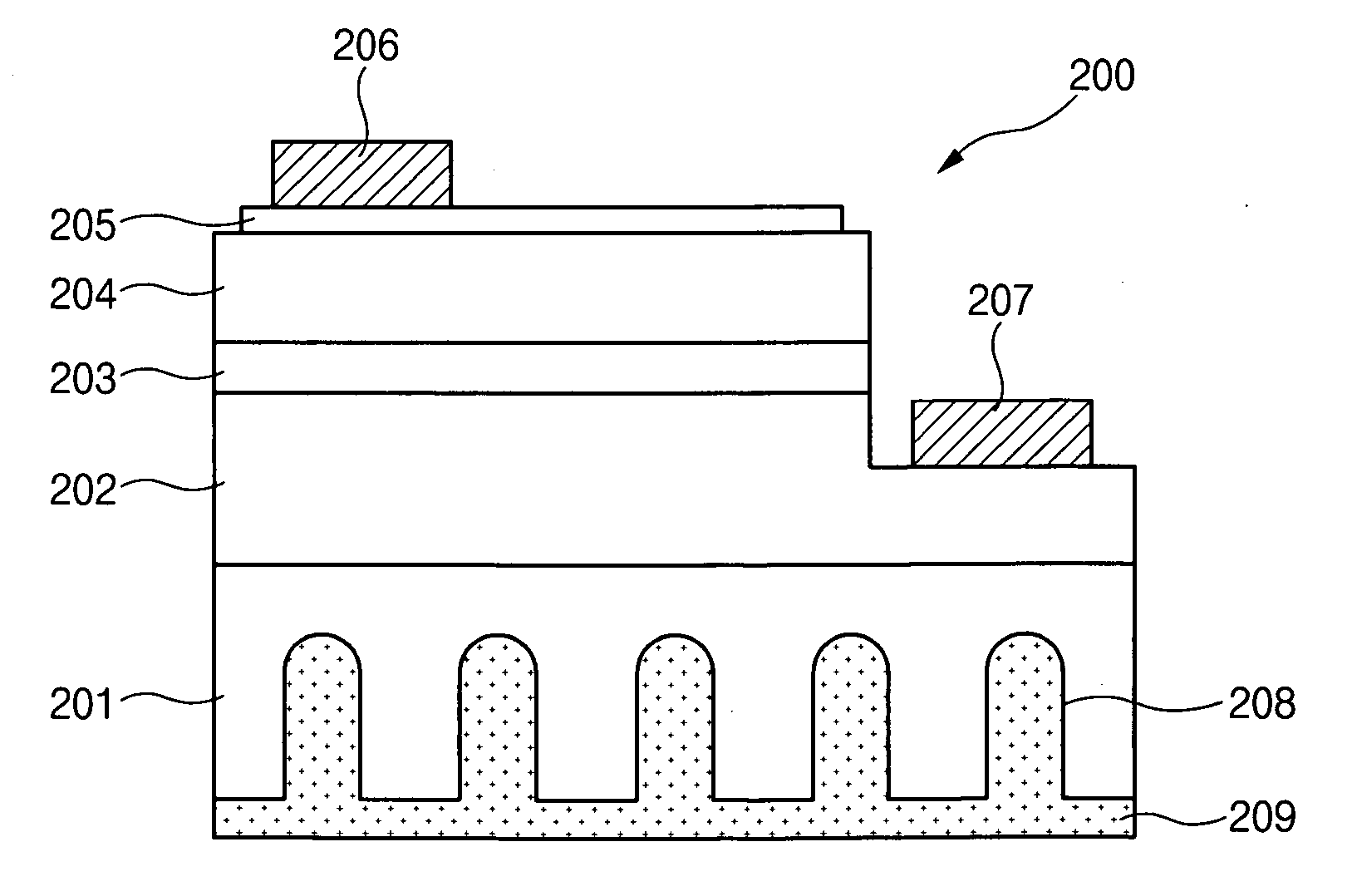
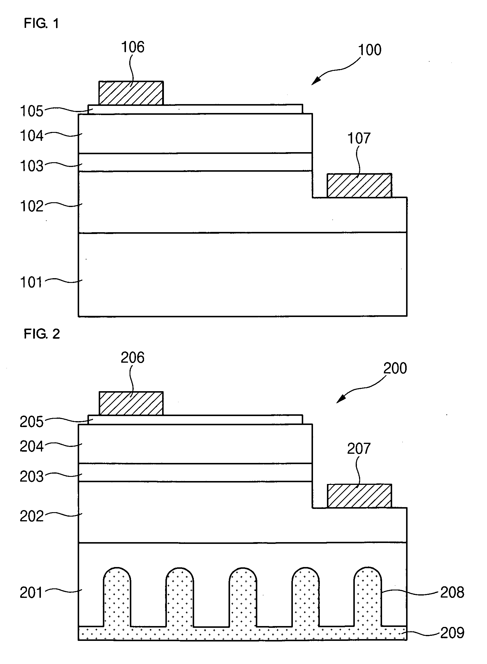
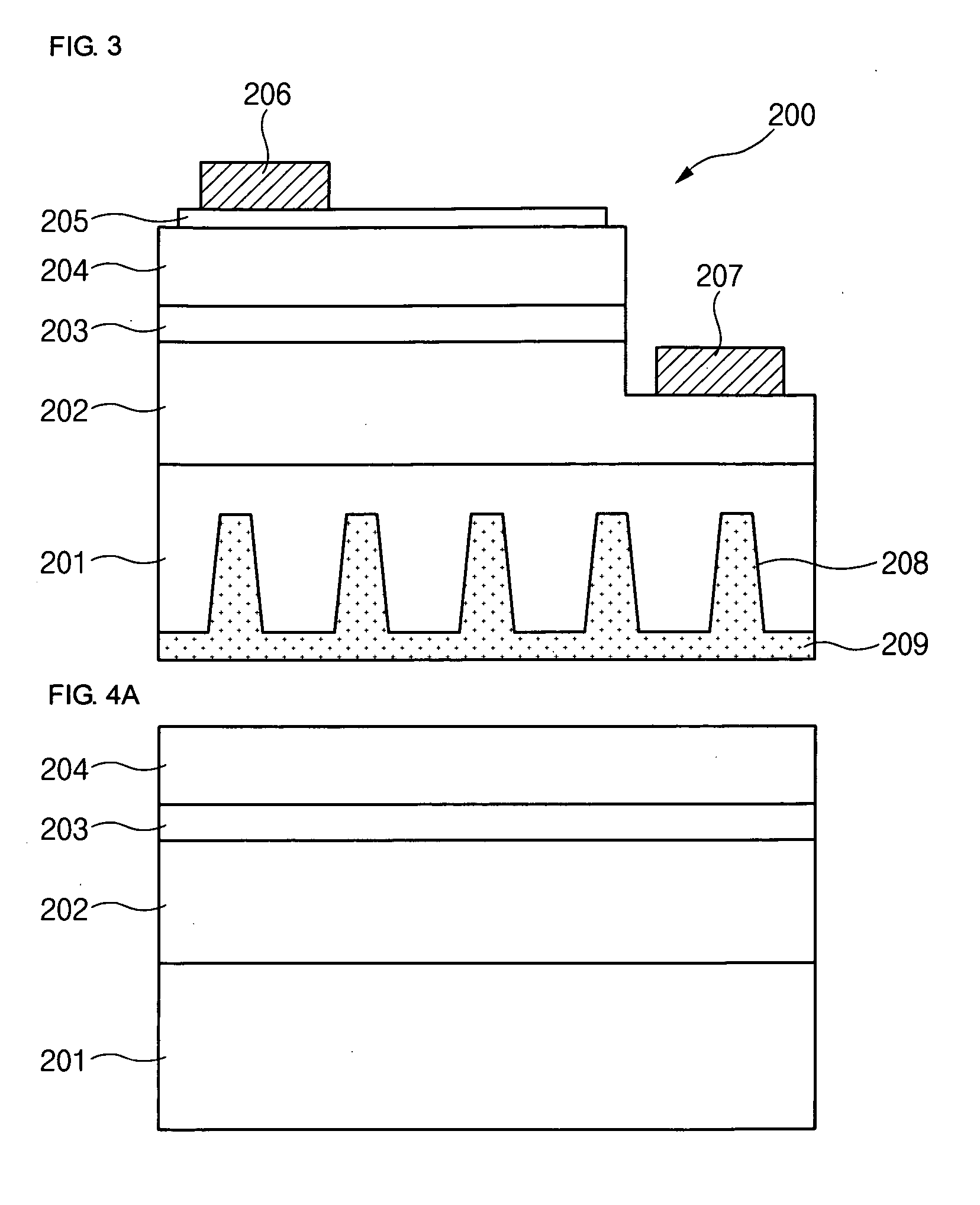
[0051] Referring to FIG. 2, the GaN based semiconductor LED 200 includes an n-type nitride semiconductor layer 202, an active layer 203, and a p-type nitride semiconductor layer 204, which are sequentially formed on a sapphire substrate 201. The sapphire substrate 201 is provided for growing a GaN based semiconductor material. A portion of the p-type nitride semiconductor layer 204 and a portion of the active layer 203 are removed by a mesa etching process, so that a predetermined upper portion of the n-type nitride semiconductor layer 202 is exposed.

[0052] The n-type nitride semiconductor layer 202, the p-type nitride semiconductor layer 20...

embodiment 2

[0072] Structure of GaN Based Semiconductor LED

[0073] Hereinafter, a GaN based semiconductor LED according to a second embodiment of the present invention will be described in detail with reference to FIG. 5. The descriptions of the same parts as the first embodiment of the present invention will be omitted for conciseness.

[0074]FIG. 5 is a sectional view of a GaN based semiconductor LED according to a second embodiment of the present invention.

[0075] Referring to FIG. 5, the GaN based semiconductor LED 300 according to the second embodiment of the present invention has the same structure as the GaN based semiconductor LED 200 according to the first embodiment of the present invention, except that a reflective layer 309 instead of the thermally conductive layer 209 is formed in a lower portion of a sapphire substrate 301 so as to fill a groove 309.

[0076] That is, the GaN based semiconductor LED 300 according to the second embodiment of the present invention includes an n-type ni...

embodiment 3

[0084] Structure of GaN Based Semiconductor LED

[0085] Hereinafter, a GaN based semiconductor LED according to the third embodiment of the present invention will be described in detail with reference to FIG. 6. The descriptions of the same parts as the first embodiment of the present invention will be omitted for conciseness.

[0086]FIG. 6 is a sectional view of a GaN based semiconductor LED according to a third embodiment of the present invention.

[0087] Referring to FIG. 6, the GaN based semiconductor LED 400 according to the third embodiment of the present invention has the same structure as the GaN based semiconductor LED 200 according to the first embodiment of the present invention, except that a reflective layer 409 having higher reflectivity than a sapphire substrate 401 is further formed between the sapphire substrate 401 with a groove 408 and a thermally conductive layer 410.

[0088] That is, the GaN based semiconductor LED 400 according to the third embodiment of the presen...


PUM

PropertyMeasurementUnit
depthaaaaaaaaaa
diameteraaaaaaaaaa
diameteraaaaaaaaaa

Abstract

A GaN based LED and a method of manufacturing the same are provided. The GaN based semiconductor LED can have an improved heat dissipation capability of a sapphire substrate, thereby preventing device characteristic from being degraded by heat and improving the luminous efficiency of the device. In the GaN based LED, a sapphire substrate has at least one groove formed in a lower portion thereof. A thermally conductive layer having higher thermal conductivity than the sapphire substrate is formed on a bottom surface of the sapphire substrate to fill the groove. An n-type nitride semiconductor layer is formed on the sapphire substrate, and an active layer and a p-type nitride semiconductor layer are sequentially formed on a predetermined portion of the n-type nitride semiconductor layer. A p-electrode and an n-electrode are formed on the p-type nitride semiconductor layer and the n-type nitride semiconductor layer, respectively.

Description

CROSS-REFERENCE TO RELATED APPLICATIONS [0001] This application claims the benefit of Korean Patent Application No. 2005-89199 filed with the Korean Industrial Property Office on Sep. 26, 2005, the disclosure of which is incorporated herein by reference. BACKGROUND OF THE INVENTION [0002] 1. Field of the Invention [0003] The present invention relates to a gallium nitride based semiconductor light emitting diode (LED) and a method of manufacturing the same. The gallium nitride based semiconductor LED can improve a heat dissipation capability of a sapphire substrate, thereby preventing device characteristic from being degraded by heat and improving the luminous efficiency of the device. [0004] 2. Description of the Related Art [0005] Because group III-V nitride semiconductors such as GaN have excellent physical and chemical properties, they are considered as essential materials of light emitting devices, for example, light emitting diodes (LEDs) or laser diode (LDs). The LEDs or LDs f...

Claims


Application Information

Patent Timeline
Patent Type & Authority Applications(United States)
IPC IPC(8): H01L33/00H01L33/42H01L33/32H01L33/60
CPCH01L33/007H01L33/0079H01L33/642H01L33/46H01L33/641H01L33/20H01L33/0093
Inventor KO, KUN YOOOH, BANG WONMIN, BOK KIPARK, HYUNG JINHWANG, SEOK MIN
Owner SAMSUNG ELECTRO MECHANICS CO LTD
Features
  • Generate Ideas
  • Intellectual Property
  • Life Sciences
  • Materials
  • Tech Scout
  • Unparalleled Data Quality
  • Higher Quality Content
  • 60% Fewer Hallucinations
Learn More