

Stacked die semiconductor package
a semiconductor and die-cutting technology, applied in the direction of solid-state devices, electric devices, basic electric elements, etc., can solve the problems of full optimization, safety risks, and packages that are bulkier than desired, and achieve the effect of reducing footprint area, efficient and rationalization
- Summary
- Abstract
- Description
- Claims
- Application Information
AI Technical Summary
Benefits of technology
Problems solved by technology
Method used
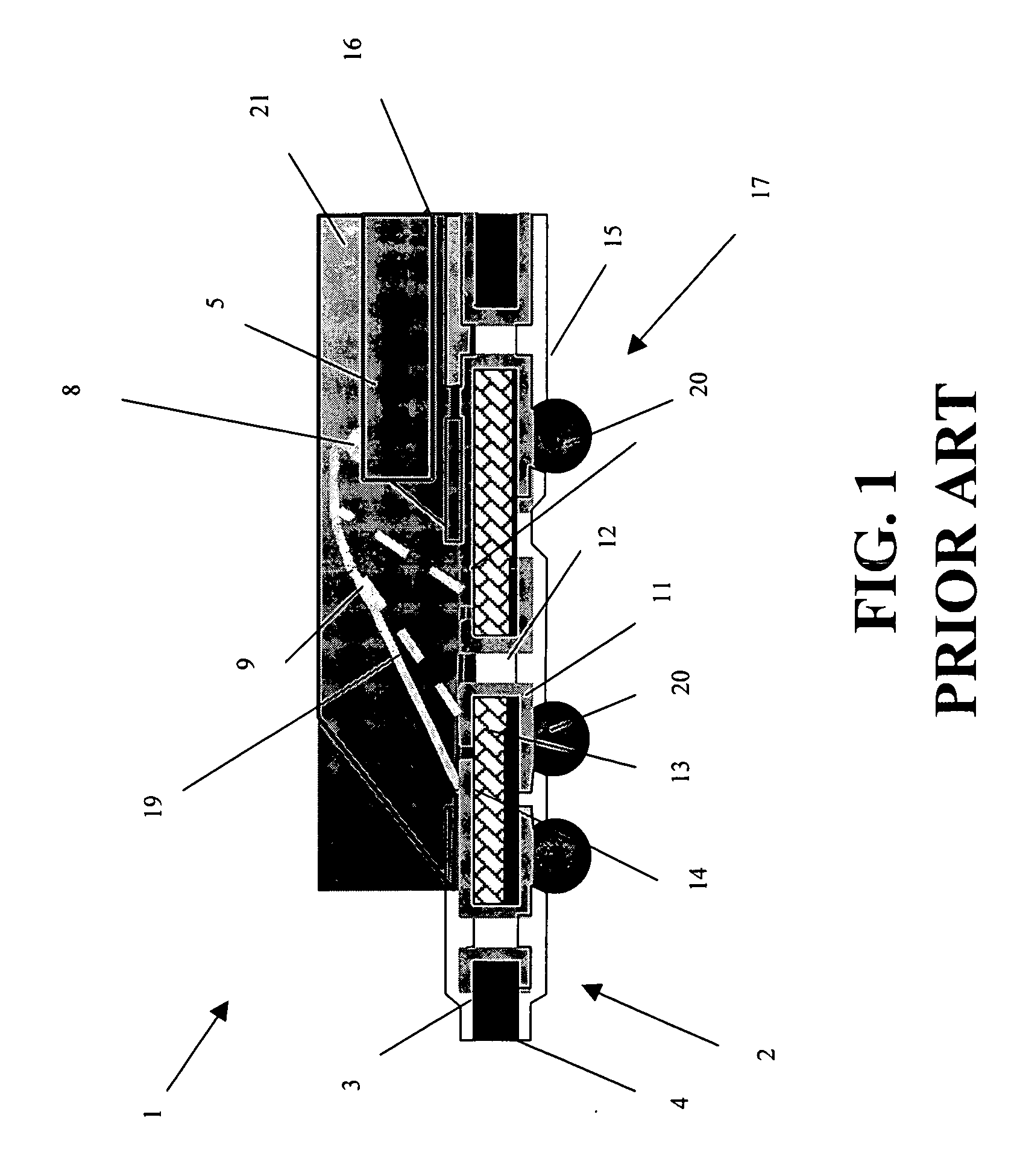
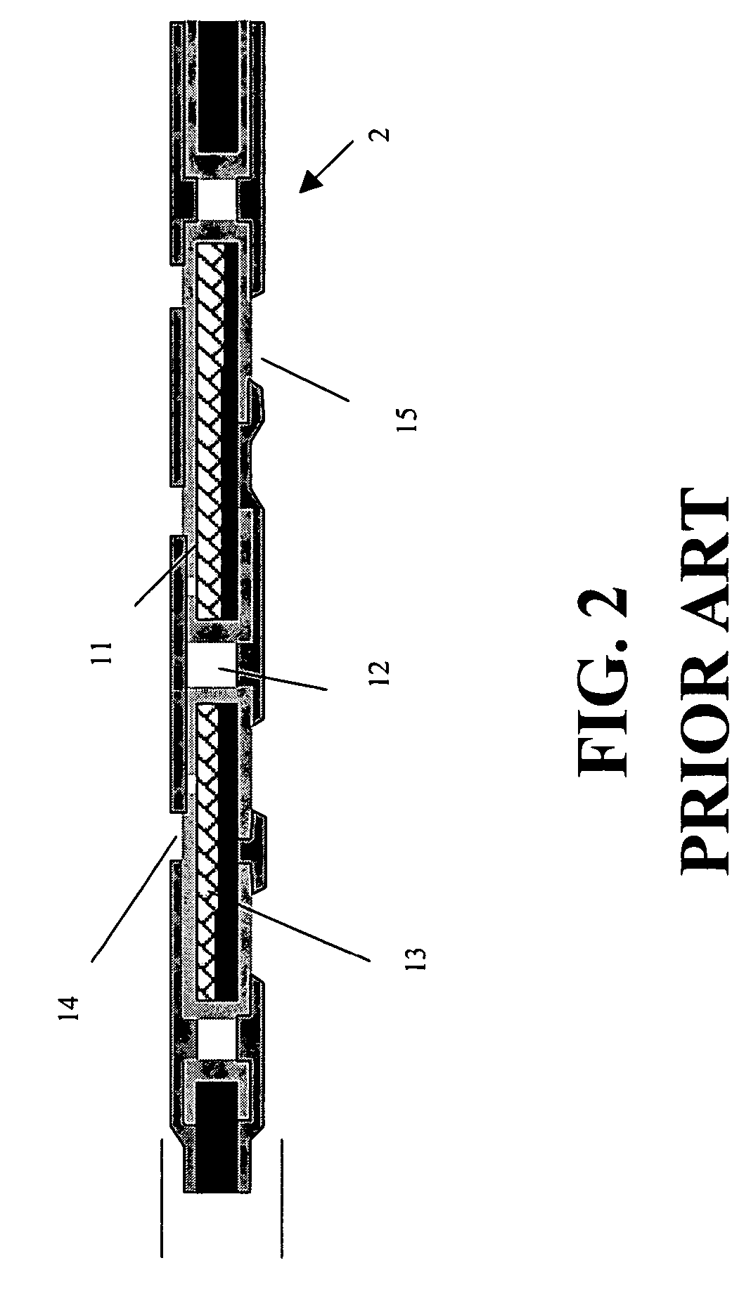
Image


Examples
example 1
Three-Die Stacked BGA Package
[0074] A BT resin substrate was covered with a layer of copper on its upper and lower surfaces and copper plated through holes were drilled through its core. A silicon die measuring 3.5×2.5×0.13 mm was attached to the upper surface of the substrate by means of glue. The wire bonding between the upper surfaces of the die and of the substrate were then done by connecting the AlSi contact pads on the upper surface of the die to the copper bond pads on the upper surface of the substrate by means of gold wires. The bond pads included a suitable finishing for wire bonding made of Ni / Au. Then, a 1.6 mm thick silicon interposer having tape on its upper and lower surfaces, was placed on top of the silicon die.
[0075] Then, the second die, having a greater footprint area than the first die (3.9×4.25×0.13 mm), and tape on its upper surface was placed on top of the interposer. Wire bonding was done for the second die, as described above for the first die. A second ...
example 2
Four-Die Stacked BGA Package
[0077] A BT resin substrate was covered with a layer of copper on its upper and lower surfaces and copper plated through holes were drilled through its core. A silicon die measuring 3.5×2.5×0.13 mm was attached to the upper surface of the substrate by means of glue. The wire bonding between the upper surfaces of the die and of the substrate were then done by connecting the AlSi contact pads on the upper surface of the die to the copper bond pads on the upper surface of the substrate by means of gold wires. The bond pads included a suitable finishing for wire bonding made of Ni / Au. Then, a 1.6 mm thick silicon interposer having tape on its upper and lower surfaces, was placed on top of the silicon die.
[0078] Then, the second die, having a greater footprint area than the first die (3.9×4.25×0.13 mm), and tape on its upper surface was placed on top of the interposer. Wire bonding was done for the second die, as described above for the first die. A second s...
PUM
 Abstract
Description
Claims
Application Information