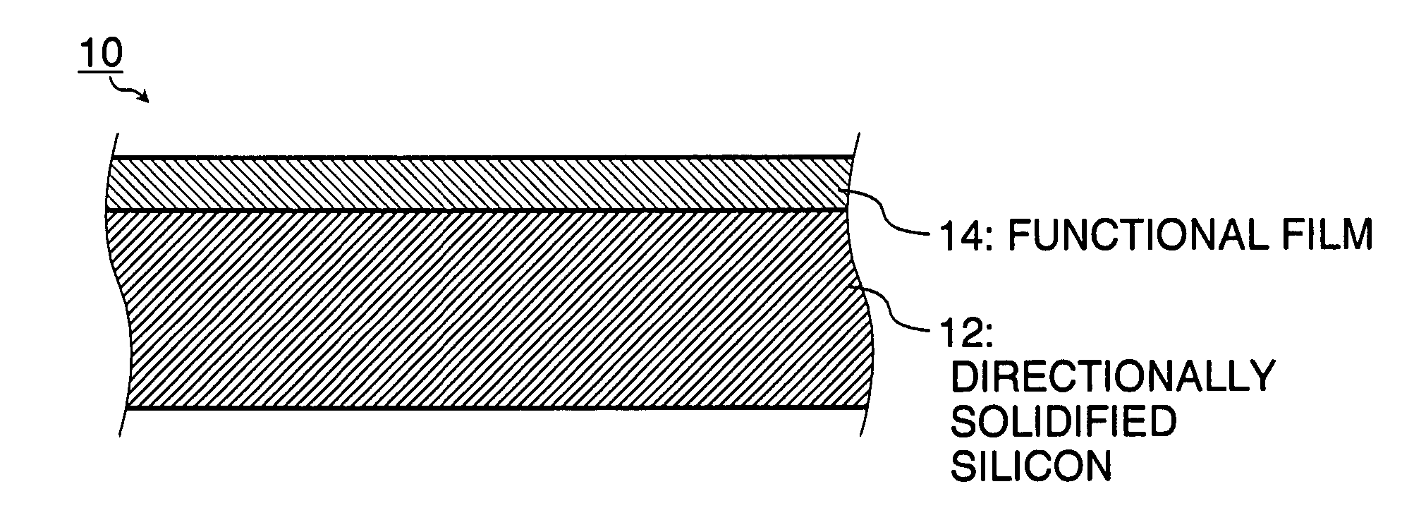
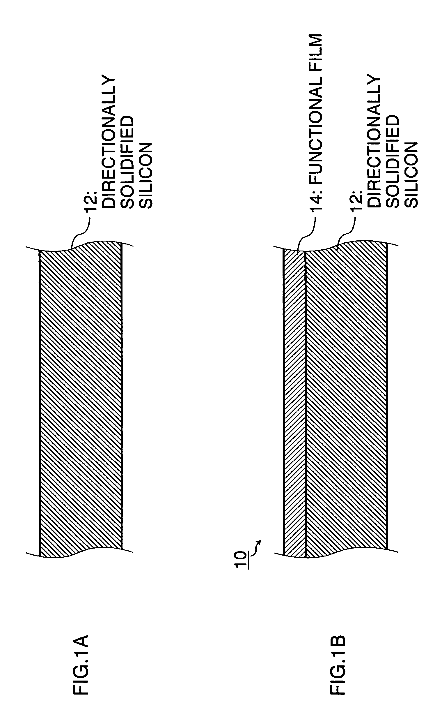
[0010] According to this aspect of the present invention, it is possible to obtain the functional structural element of a
large size by using the directionally solidified silicon substrate, which can readily be formed to a
large size. Moreover, since the price per unit surface area of the directionally solidified silicon substrate is inexpensive, then it is possible to reduce the cost of the functional structural element. Furthermore, by forming the directionally solidified silicon substrate to a
large size, it is possible to manufacture a large amount of functional structural elements, from one substrate of directionally solidified silicon, by one manufacturing process, and therefore it is possible to reduce the
unit cost of the functional structural element.
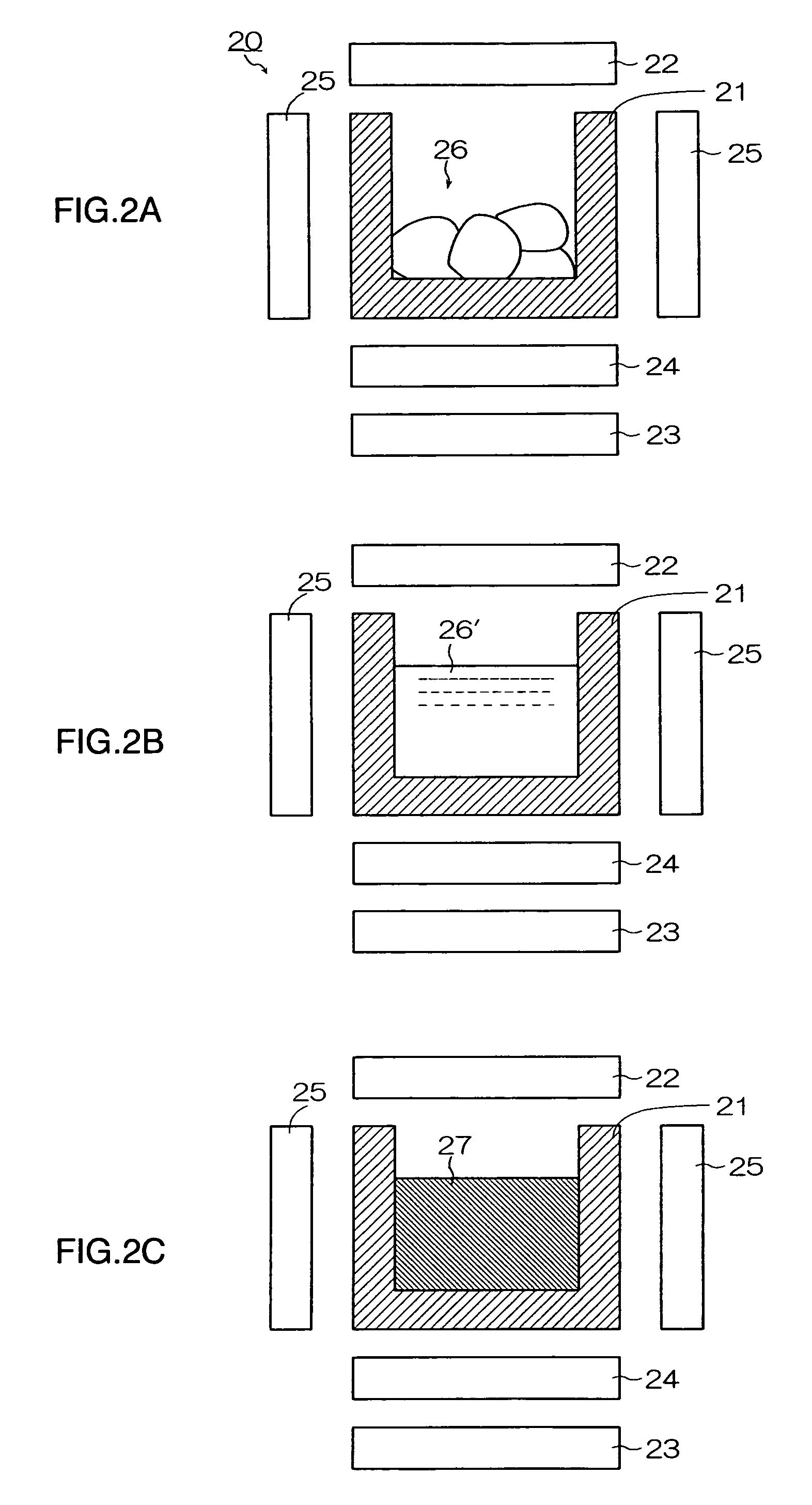
[0013] According to this aspect of the present invention, by forming the buffer layer between the directionally solidified silicon substrate and the functional structural body, it is possible to suppress
diffusion of
oxygen or the elements of the functional material to the surface of the directionally solidified silicon substrate, compared to a case where the functional material is deposited directly onto the surface of the directionally solidified silicon substrate. Therefore, it is possible to deposit the functional material more stably, and furthermore, it is also possible to improve the quality of the functional structural body. Moreover, in the case where the directionally solidified silicon substrate and the functional structural body have different lattice constants, it is possible to improve the quality of the functional structural body by providing the buffer layer of a material having the intermediate characteristics between those of directionally solidified silicon and the functional material (for example, a material having a
lattice constant between that of directionally solidified silicon and that of the functional material).
[0018] According to this aspect of the present invention, it is possible to obtain the functional structural element of a large size by using a directionally solidified silicon substrate, which can readily be formed to a large size. Furthermore, since the price per unit surface area of the directionally solidified silicon substrate is inexpensive, then it is possible to reduce the cost of the functional structural element. Moreover, by forming the directionally solidified silicon substrate to a large size, it is possible to manufacture a large amount of functional structural elements, from one substrate of directionally solidified silicon, by one manufacturing process, and therefore it is possible to reduce the
unit cost of the functional structural element.
[0020] According to this aspect of the present invention, by forming the buffer layer between the directionally solidified silicon substrate and the functional structural body, it is possible to suppress
diffusion of
oxygen or the elements of the functional material to the surface of the directionally solidified silicon substrate, compared to a case where the functional material is deposited directly onto the surface of the directionally solidified silicon substrate. Therefore, it is possible to deposit the functional material more stably, and furthermore, it is also possible to improve the quality of the functional structural body. Moreover, in the case where the directionally solidified silicon substrate and the functional structural body have different lattice constants, it is possible to improve the quality of the functional structural body by providing the buffer layer of a material having the intermediate characteristics between those of directionally solidified silicon and the functional material (for example, a material having a
lattice constant between that of directionally solidified silicon and that of the functional material).
[0023] According to the present invention, it is possible to obtain the functional structural element of a large size by using the directionally solidified silicon substrate, which can readily be formed to a large size. Moreover, since the price per unit surface area of the directionally solidified silicon substrate is inexpensive, then it is possible to reduce the cost of the functional structural element. Further, by forming the directionally solidified silicon substrate to a large size, it is possible to manufacture a large amount of functional structural elements, from one substrate of directionally solidified silicon, by one manufacturing process, and therefore it is possible to reduce the
unit cost of the functional structural element. Furthermore, in the case where the directionally solidified silicon substrate and the functional structural body have significantly different lattice constants, it is possible to improve the quality of the functional structural body by providing a buffer layer of a material having intermediate characteristics between those of directionally solidified silicon and the functional material (for example, a material having a
lattice constant between that of directionally solidified silicon and that of the functional material).

