

Electronic device, semiconductor device using same, and method for manufacturing semiconductor device
- Summary
- Abstract
- Description
- Claims
- Application Information
AI Technical Summary
Benefits of technology
Problems solved by technology
Method used
Image

Examples
Embodiment Construction
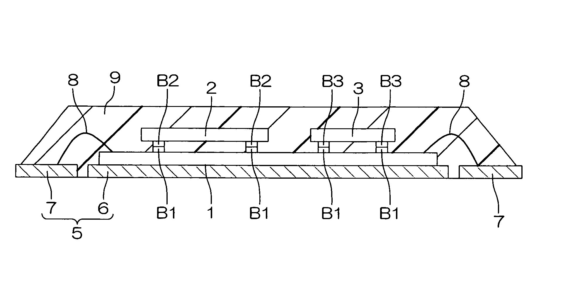
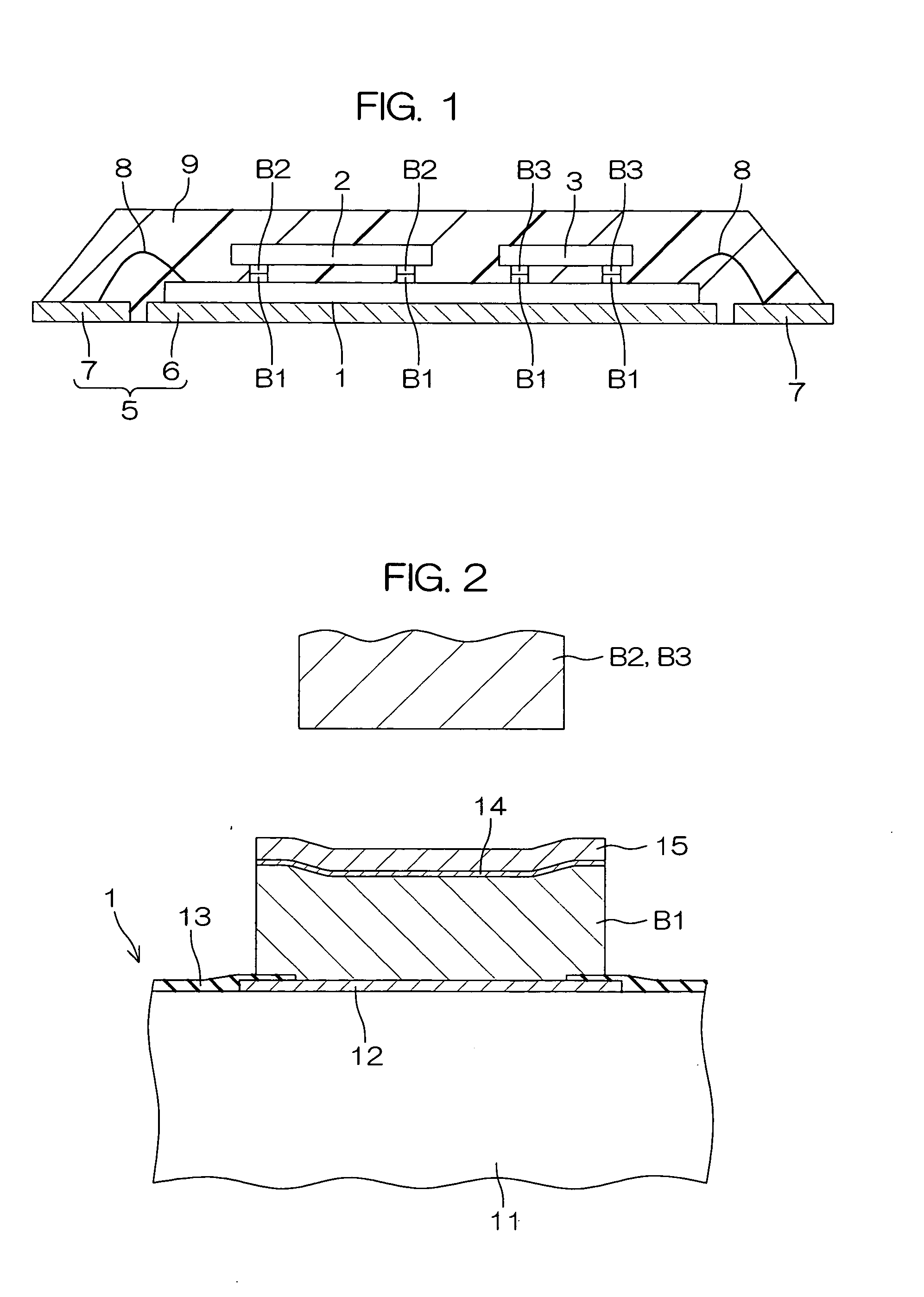
[0034]FIG. 1 is a schematic sectional view for explaining the construction of a semiconductor device according to one embodiment of the present invention. The semiconductor device has a so-called chip-on-chip structure, which includes a primary chip 1 and secondary chips 2, 3 bonded onto the primary chip 1. The primary chip 1 and the secondary chips 2, 3 are semiconductor chips (e.g., silicon chips). The secondary chips 2, 3 are bonded to the primary chip 1 in face-to-face relation with their active surfaces opposed to an active surface (a surface on an active region side formed with elements) of the primary chip 1. More specifically, the primary chip 1 is die-bonded onto an island 6 of a lead frame 5 with its active surface upward, and the secondary chips 2, 3 are bonded onto an upper surface of the primary chip 1 with their faces down. The primary chip 1 has external connection pads (not shown) provided on the active surface thereof, and the pads are electrically connected to lead...
PUM
 Abstract
Description
Claims
Application Information