Eureka AIR delivers breakthrough ideas for toughest innovation challenges, trusted by R&D personnel around the world.

Circuit and method for driving an array of light emitting pixels

Active Publication Date: 2007-04-12
IGNIS INNOVATION
View PDF26 Cites 271 Cited by
  • Summary
  • Abstract
  • Description
  • Claims
  • Application Information

AI Technical Summary

Benefits of technology

[0017] Advantages of the present invention include the ability to provide a stable current to the light emitting diode over time, thereby maintaining image quality. Moreover, the combination of the external current feedback for pixel programming and luminance feedback for data signal preprocessing provides brightness control and compensation despite instability and non-uniformity in pixels. The circuits occupy a small area and are voltage programmed with voltage feedback. The use of voltage for programming and feedback improves the programming speed, which is necessary for large area displays and TVs.

Problems solved by technology

Since the characteristic parameters of a TFT, particularly, the threshold voltage under bias stress, vary by time, and such changes may differ from pixel to pixel, the induced image distortion may be unacceptably high.
A drawback of the current programming method is that it is slow, particularly for low programming current levels, due to the large line capacitance.
One drawback of the disclosed method is that the control signal is a current, which can limit the programming speed.
Another drawback of the method is that the anode and cathode electrode of each OLED have to be patterned, which creates reliability concerns in the currently used OLED fabrication process.
A drawback of the disclosed method is that every pixel requires a photo-sensor that is optically coupled to the OLED.
This results in integration issues.
Another drawback is that the low level of the feedback signal generated by a photo-sensor may lead to the poor signal-noise ratio, thereby narrowing the dynamic range of the system.

Method used


Image

  • Circuit and method for driving an array of light emitting pixels
  • Circuit and method for driving an array of light emitting pixels
  • Circuit and method for driving an array of light emitting pixels

Examples


Embodiment Construction

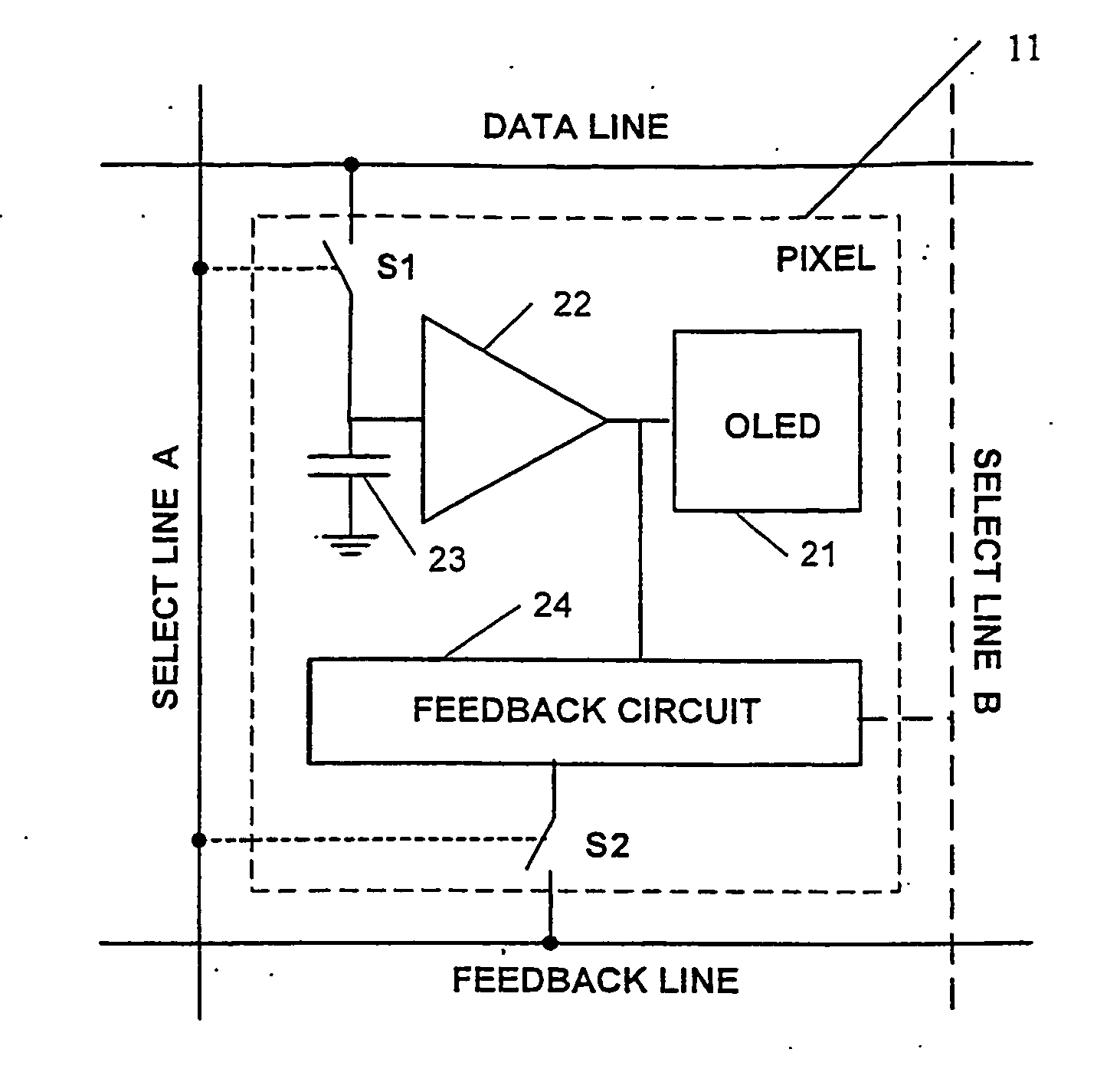
[0038] The present invention encompasses a technique for driving of columns of pixels where each pixel comprises a light emitting element, in particular, an organic light emitting diode (OLED).

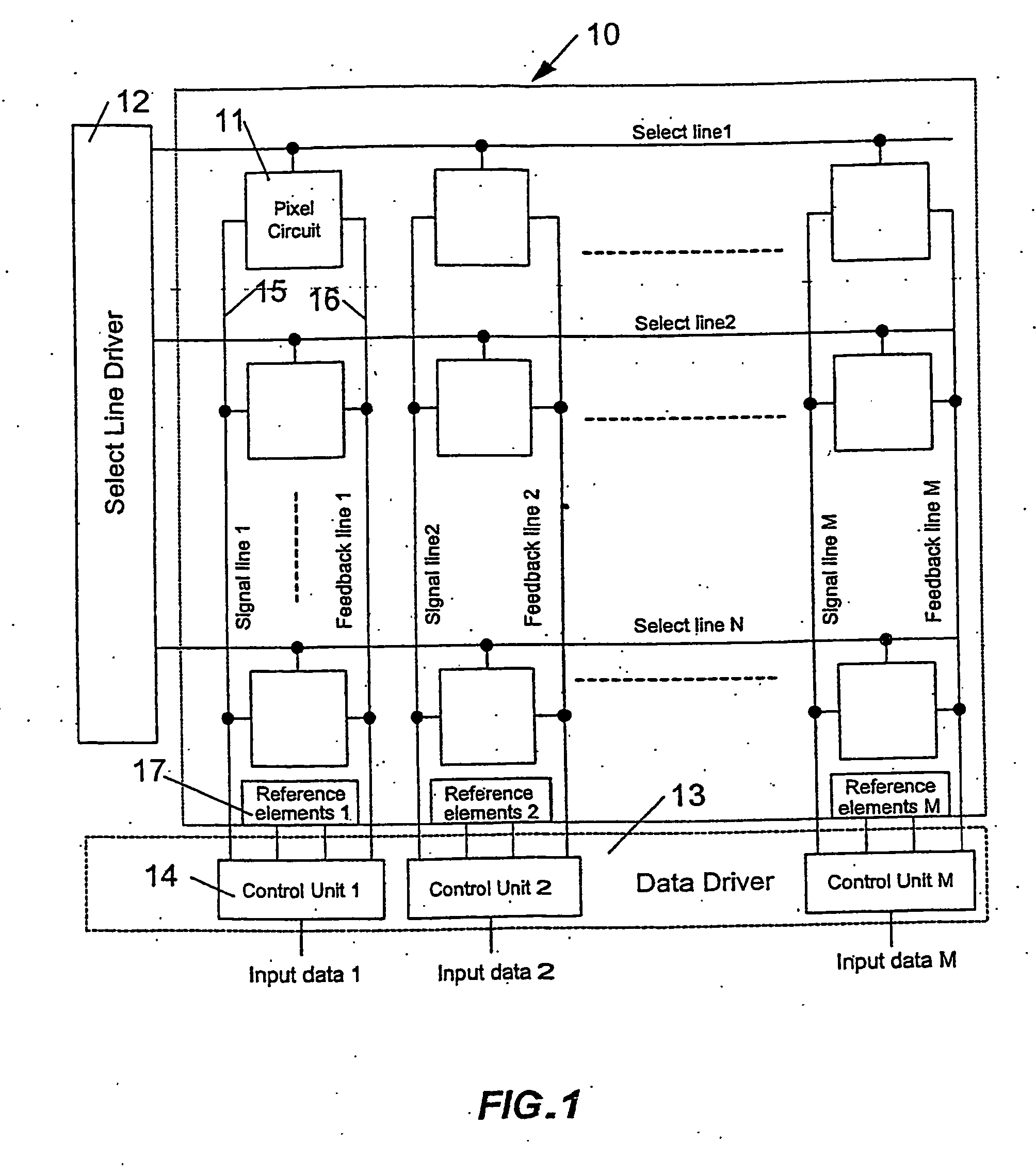
[0039]FIG. 1 presents a display device having a feedback control-system architecture 10 and an array of addressable pixels 11. The pixels 11 are controlled by a select line driver 12 and data driver 13. As shown in FIG. 1, a separate feedback control unit 14 is provided on each column line of the array. The feedback control unit 14 of a given column is connected to each pixel in the column via a signal line 15 and a feedback line 16. A block of reference elements 17, located on the display substrate, may also be provided. The block of the reference elements 17 includes some elements of the pixel circuit for input signal corrections and may also include a photo-sensor that is optically coupled to a light emitting element to implement a luminance feedback.

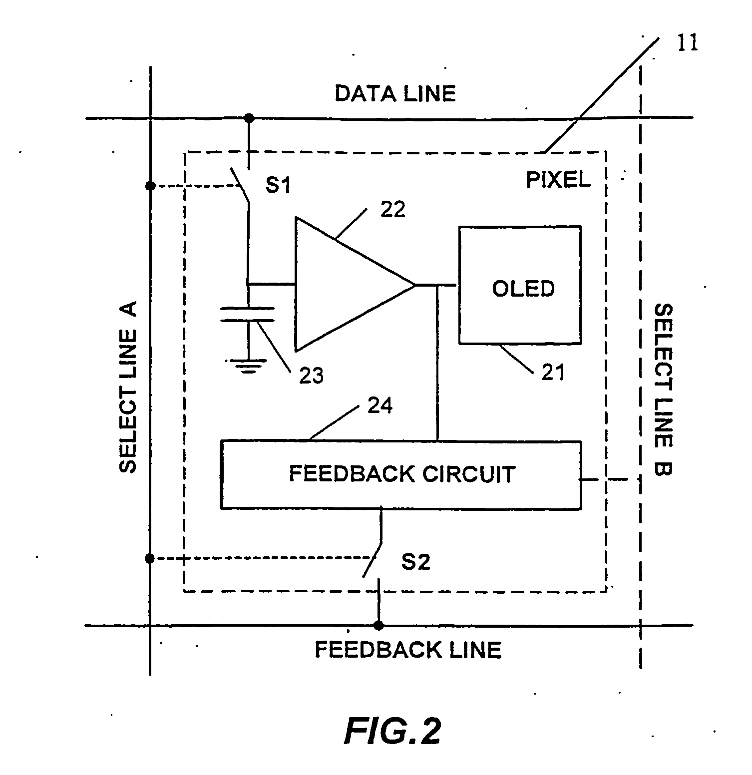
[0040] The structure of a given pixel ...


PUM


Abstract

A technique for driving a column of pixels that include light emitting elements is presented. The technique incorporates feedback data provided from feedback data sources connected to the data line and to feedback line of the array, pixel driving circuit with feedback path. The technique can also include block of the reference elements for input signal corrections.

Description

FIELD OF INVENTION [0001] The present invention generally relates to a light emitting device display techniques, and more particularly, to a technique for driving light emitting elements that uses a feedback architecture during programming to compensate for instability and non-uniformity of the pixels. BACKGROUND OF THE INVENTION [0002] Recently active-matrix organic light-emitting diode (OLED) displays have become more attractive due to advantages over conventional liquid crystal flat displays. These advantages include the ability to fabricate OLED displays at a relatively low cost and high efficiency. Further the displays do not require backlighting and provide a wide viewing angle. [0003] An active-matrix organic light-emitting diode (AMOLED) display compromises an array of rows and columns of pixels, each having an OLED and some active devices such as thin film transistors. Since OLEDs are current driven devices the pixel circuit of an AMOLED should be capable of providing an ac...

Claims


Application Information

Patent Timeline
IPC IPC(8): G09G3/30G09F9/33G09G3/3208G09G3/3225H05B44/00
CPCG09G3/3241H05B37/0209G09G2300/0842G09G2300/0417G09G3/3283H05B45/10Y02B20/30H05B45/60G09G3/3266G09G2300/0809G09G2300/0819G09G3/325G09G2320/0646
Inventor NATHAN, AROKIAVYGRANENKO, YURIYJAFARABADIASHTIANI, SHAHINSERVATI, PEYMAN
Owner IGNIS INNOVATION
Why Eureka
Eureka Blog
Learn More