

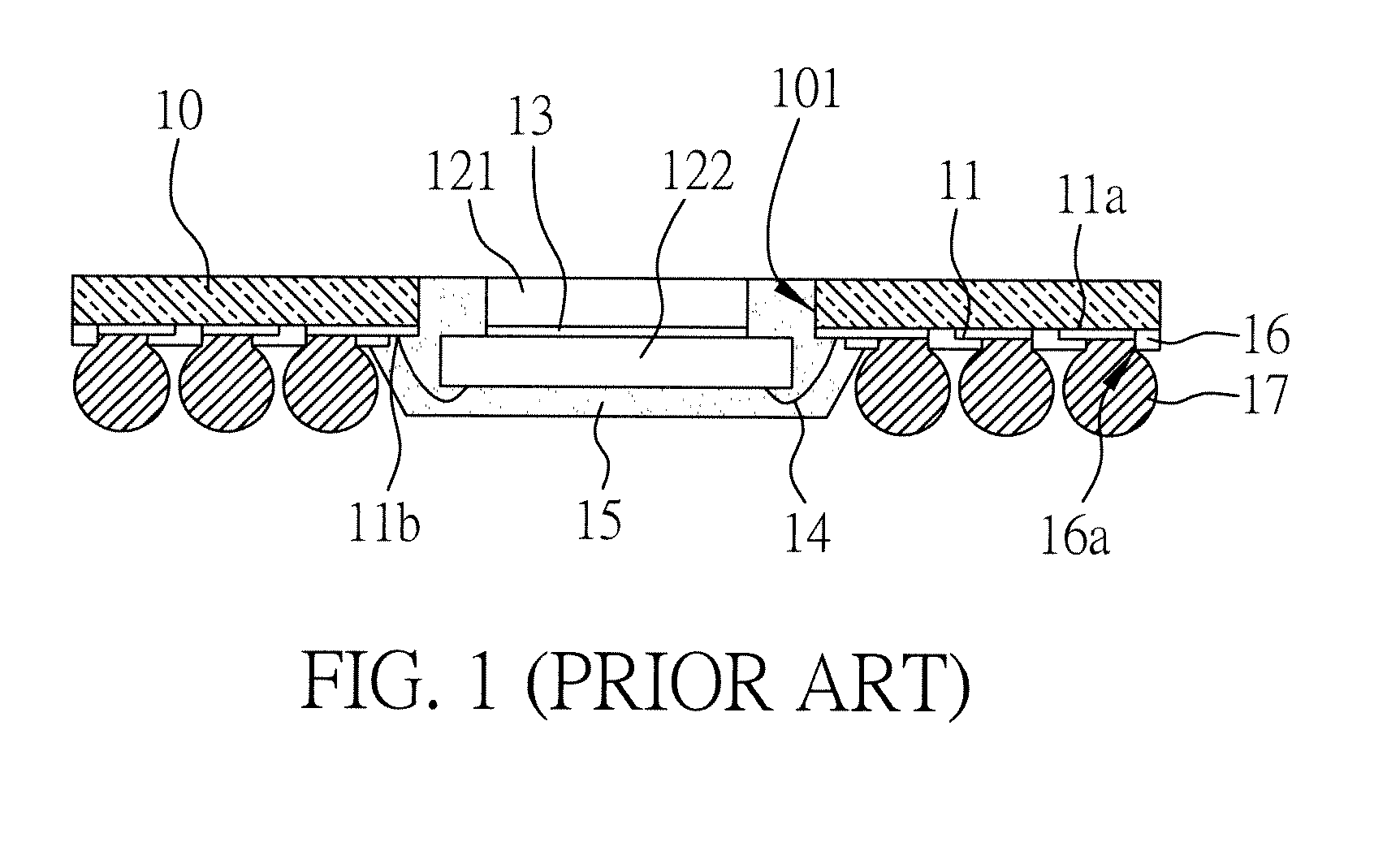
Stack Structure of Carrier Board Embedded with Semiconductor Components and Method for Fabricating the same
a carrier board and semiconductor technology, applied in the direction of printed circuit manufacturing, printed circuit components, printed circuit components, etc., can solve the problems of cdbga not having better electricity and modularization functionality, cdbga having too thick structure, and complicated manufacturing process to manufacture cdbga, so as to simplify the semiconductor packaging process, reduce the dimension of the modular structure, and efficiently use the space of the carrier board
- Summary
- Abstract
- Description
- Claims
- Application Information
AI Technical Summary
Benefits of technology
Problems solved by technology
Method used
Image

Examples
Embodiment Construction
[0020] The following illustrative embodiments are provided to illustrate the disclosure of the present invention, these and other advantages and effects can be apparently understood by those in the art after reading the disclosure of this specification. The present invention can also be performed or applied by other different embodiments. The details of the specification may be on the basis of different points and applications, and numerous modifications and variations can be devised without departing from the spirit of the present invention.
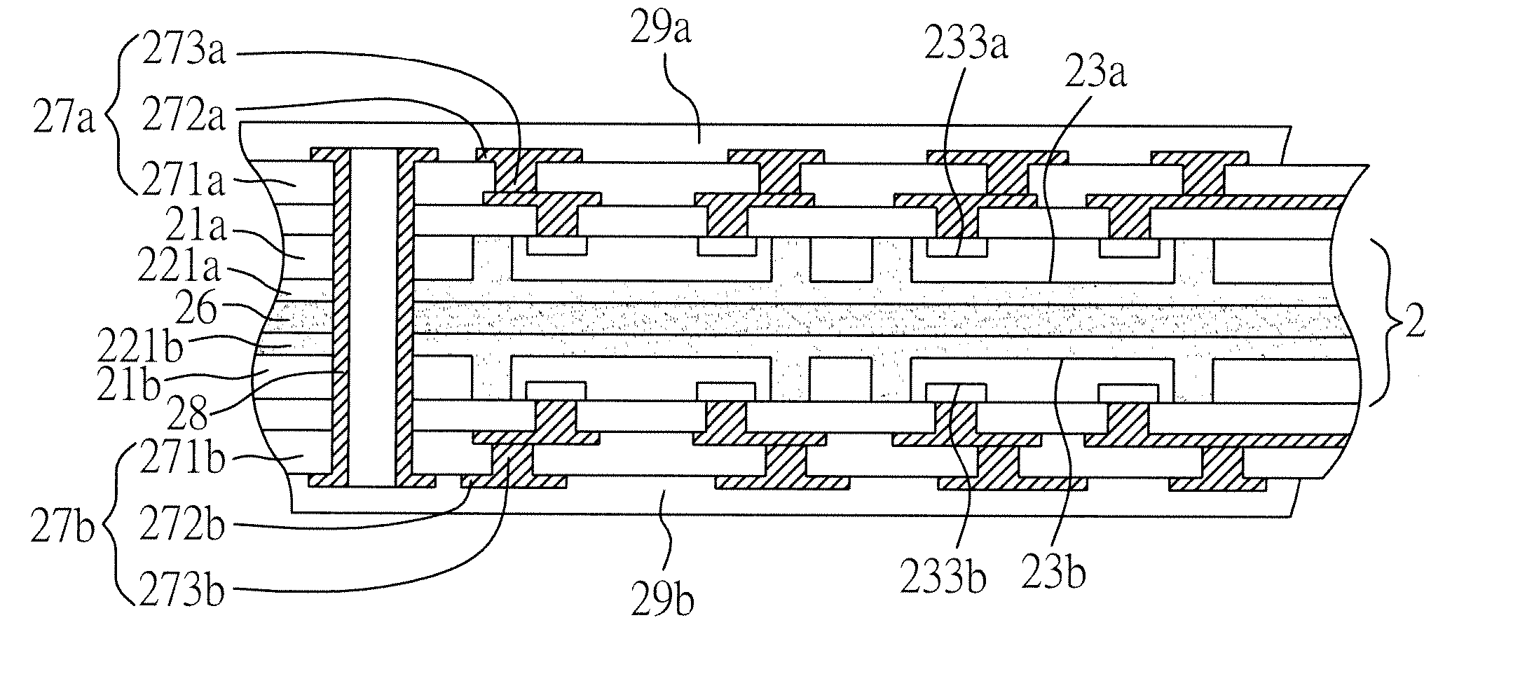
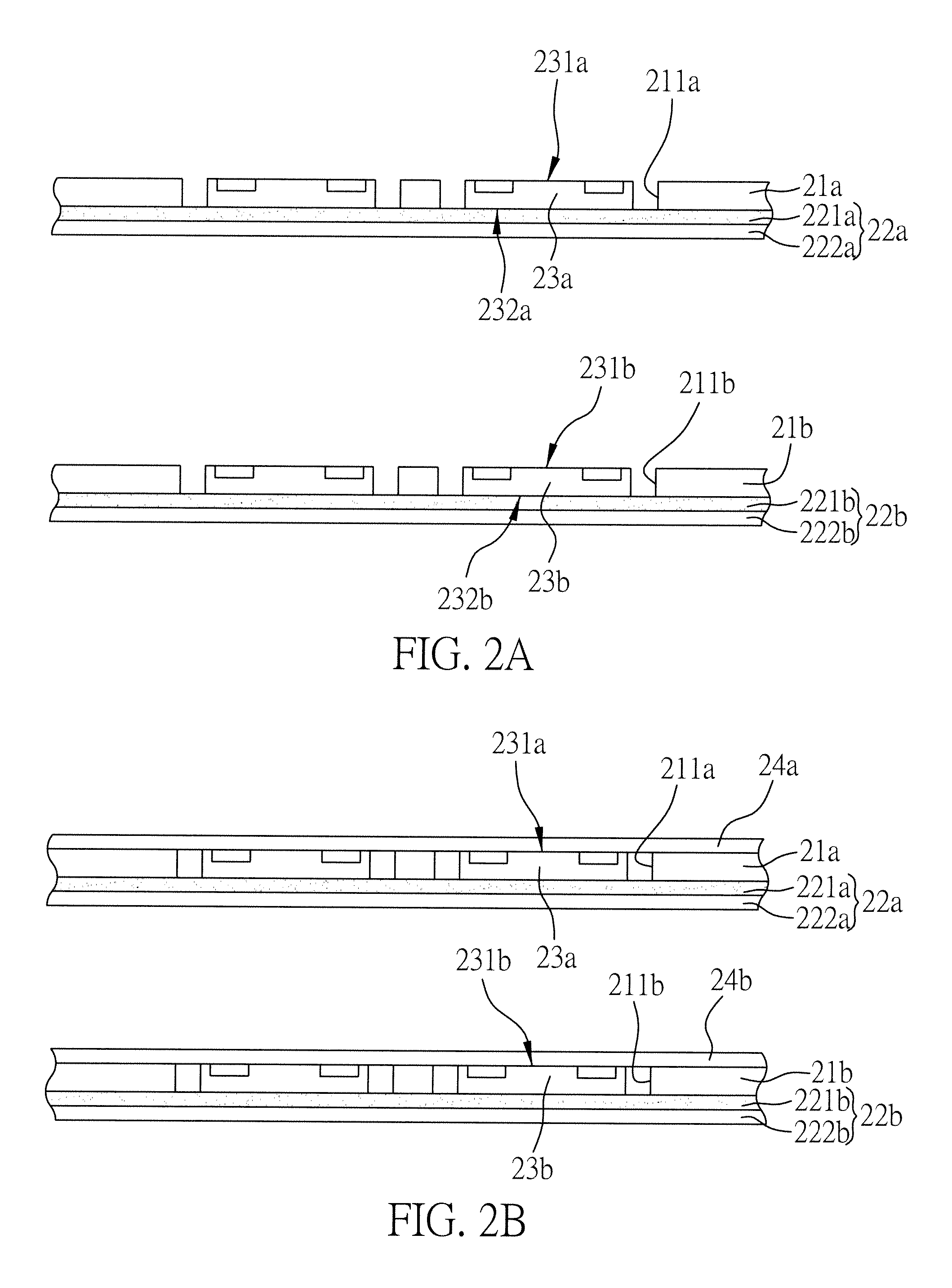
[0021]FIGS. 2A to 2G are used for demonstrating a method for fabricating a stack structure of a carrier board embedded with semiconductor components according to the present invention.
[0022] Please refer to FIG. 2A, which shows a first carrier board 21a and a second carrier board 21b of the present invention. Two through holes 211a and 211b are formed in the first and second carrier boards 21a and 211b respectively. Both the first and second c...
PUM
| Property | Measurement | Unit |
|---|---|---|
| dielectric | aaaaa | aaaaa |
| semiconductor | aaaaa | aaaaa |
| conductive | aaaaa | aaaaa |
Abstract
Description
Claims
Application Information