Methods and apparatus for process abatement

a technology of process abatement and abatement method, which is applied in the direction of lighting and heating apparatus, separation processes, machines/engines, etc., can solve the problems of difficult breakdown or reduction of sub>2 /sub> to non-toxic forms, and the exposure to as little as 1 ppm of f can be hazardous to humans and the environmen

Inactive Publication Date: 2007-04-19
APPLIED MATERIALS INC
View PDF13 Cites 31 Cited by
  • Summary
  • Abstract
  • Description
  • Claims
  • Application Information

AI Technical Summary

Problems solved by technology

These gases are toxic to humans and hazardous to the environment.
Extended exposure to as little as 1 ppm of F2 can be hazardous, and F2 is difficult to breakdown or reduce to non-toxic forms.
However, this techniqu...

Method used


Image

  • Methods and apparatus for process abatement
  • Methods and apparatus for process abatement
  • Methods and apparatus for process abatement

Examples


Embodiment Construction

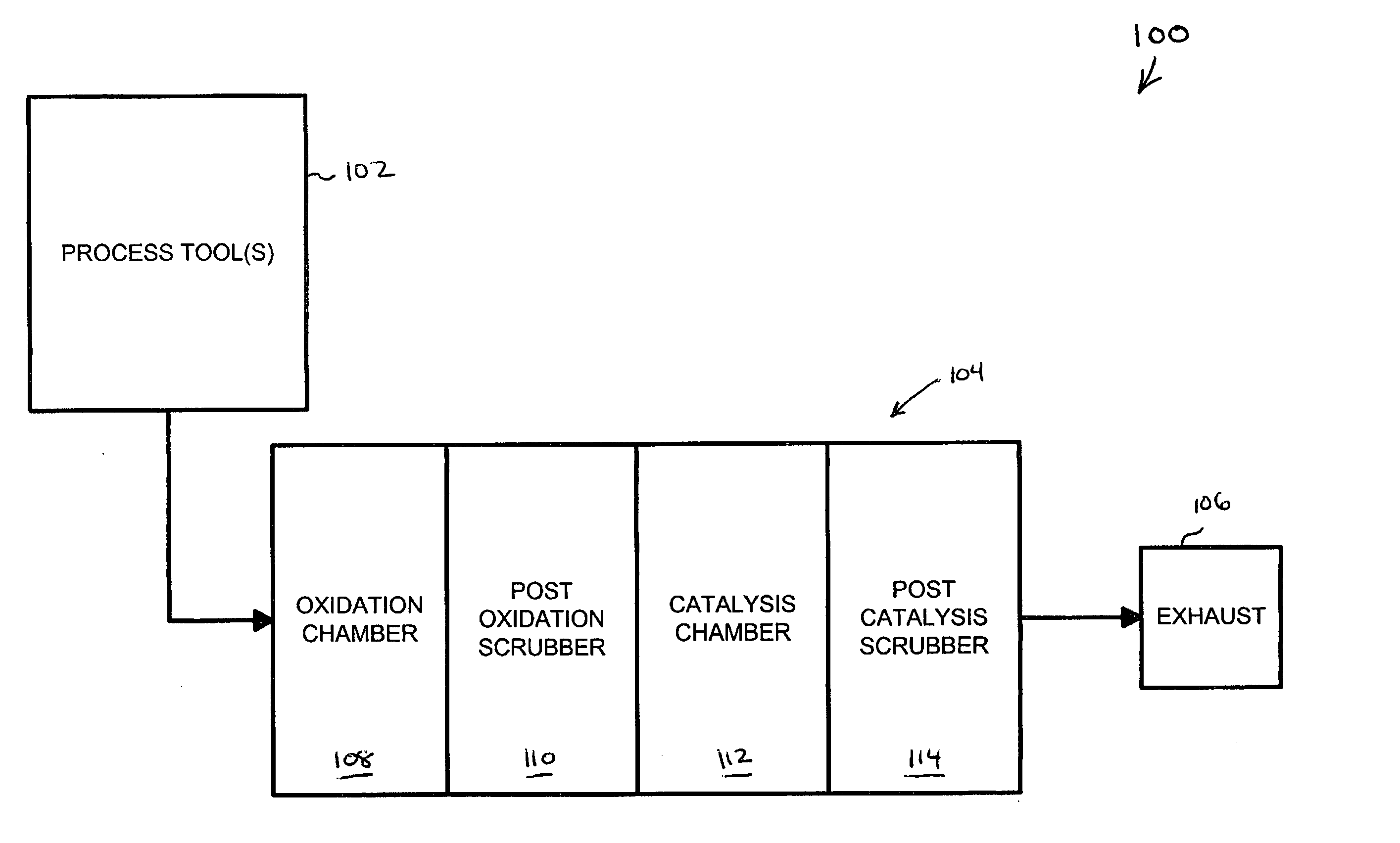
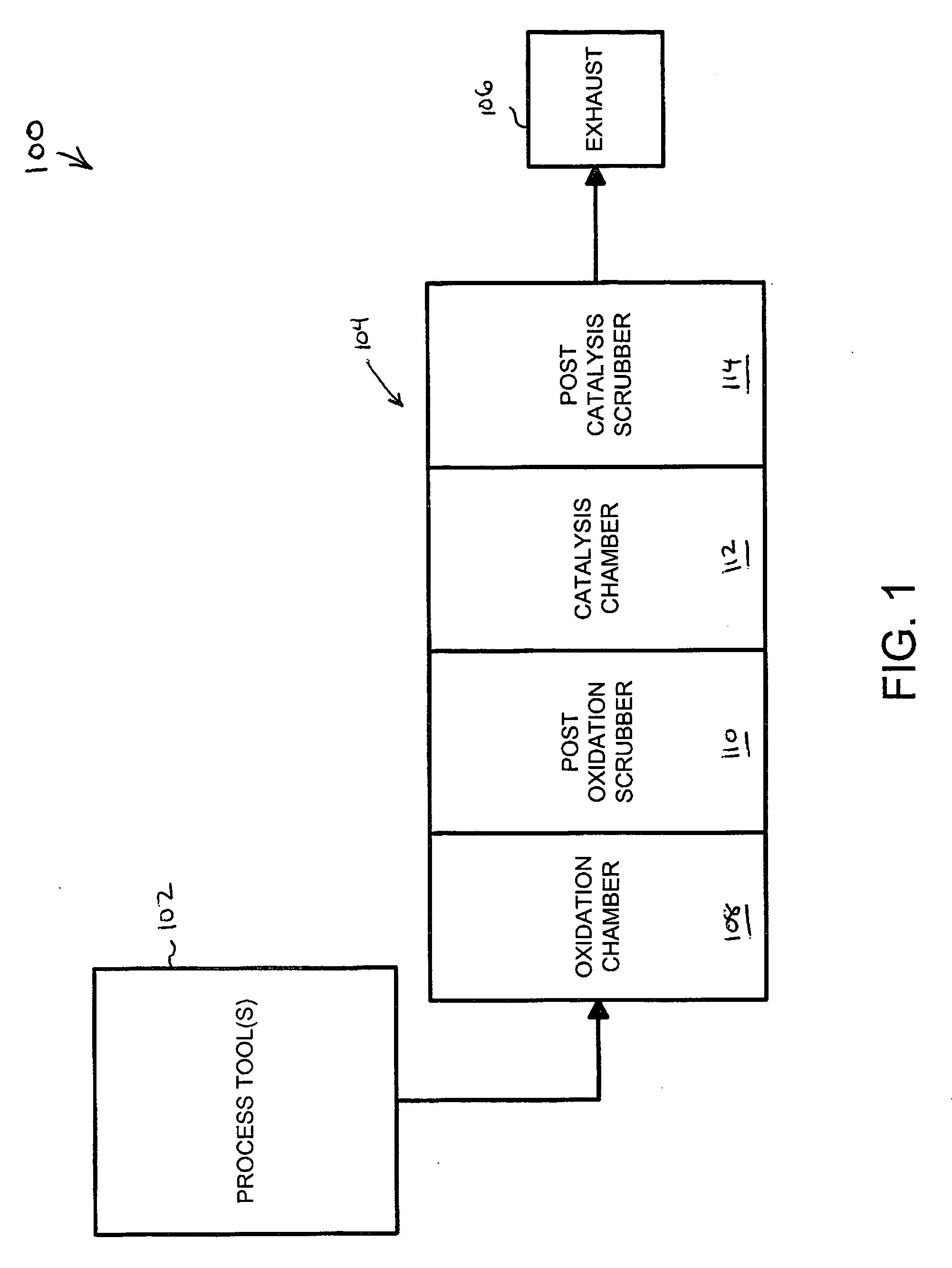
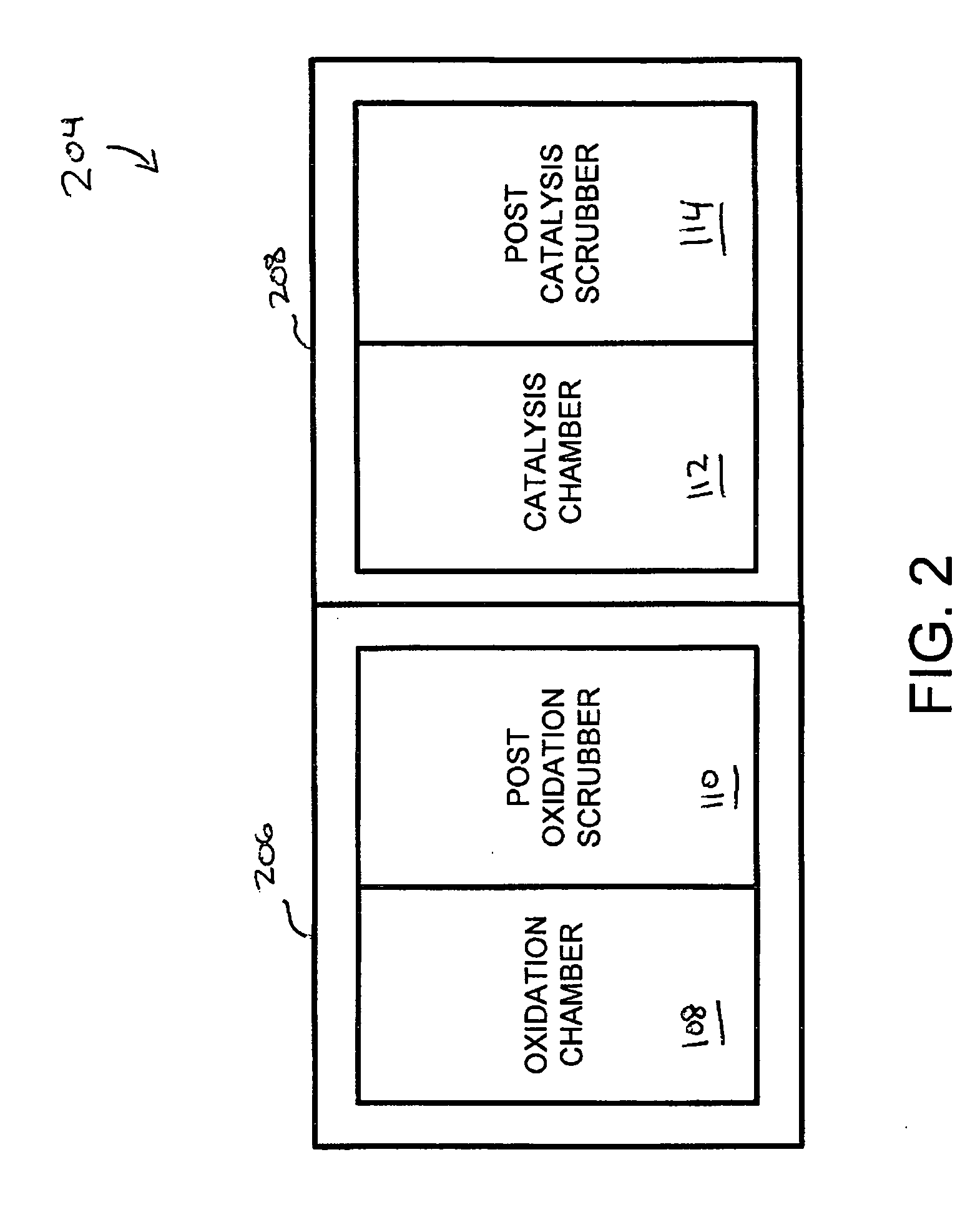
[0020] The present invention provides methods and apparatus for abating semiconductor device manufacturing equipment. For example, the present invention may be employed to abate perfluorocompounds (PFCs), hazardous air pollutants (HAPs), volatile organic compounds (VOCs) or other similar materials generated during semiconductor device manufacturing processes and / or during cleaning of semiconductor device manufacturing equipment such as processes and / or chambers associated with plasma enhanced chemical vapor deposition (PECVD), low K or high K deposition, high density plasma CVD (HDPCVD), sub-atmospheric CVD (SACVD), low pressure CVD (LPCVD), metal CVD (MCVD), etch, epitaxial growth, rapid thermal processing (RTP), implant, etc. In one exemplary embodiment, the present invention may be employed to abate PFCs generated during the cleaning of a CVD chamber.

[0021] In one or more embodiments of the invention, abatement is improved by combining electric oxidation, thermal catalysis and w...


PUM

PropertyMeasurementUnit
Pressureaaaaaaaaaa

Abstract

In a first aspect, a first abatement apparatus is provided. The first abatement apparatus includes (1) an oxidation unit adapted to receive an effluent stream from a semiconductor device manufacturing chamber; (2) a first water scrubber unit adapted to receive the effluent stream from the oxidation unit; and (3) a catalysis unit adapted to receive the effluent stream from the first water scrubber unit. Numerous other aspects are provided.

Description

[0001] The present application claims priority from U.S. Provisional Patent Application Ser. No. 60 / 690,340, filed Jun. 13, 2005 (Attorney Docket No. 10324 / L), which is hereby incorporated by reference herein in its entirety.FIELD OF THE INVENTION [0002] The present invention relates generally to semiconductor device manufacturing, and more particularly to methods and apparatus for abating semiconductor device manufacturing equipment. BACKGROUND OF THE INVENTION [0003] Fluorocarbon, chlorofluorocarbon, hydrocarbon, and other fluorine containing gases are used in, or formed as a byproduct during, the manufacture of active and passive electronic circuitry in process chambers. These gases are toxic to humans and hazardous to the environment. In addition, they may also strongly absorb infrared radiation and have high global warming potentials. Especially notorious are persistent fluorinated compounds or perfluorocompounds (PFCs) which are long-lived, chemically stable compounds that hav...

Claims


Application Information

Patent Timeline
IPC IPC(8): B01D53/34B01D53/46B01D53/86
CPCB01D53/68B01D53/70B01D53/75B01D53/78B01D53/8659B01D53/8662B01D53/8678B01D2257/204B01D2257/206B01D2257/2064B01D2257/2066B01D2257/708B01D2258/0216Y02C20/30B01D53/00
Inventor RAOUX, SEBASTIENKINGSTON, BRIANCURRY, MARKCLARK, DANIELVERMEULEN, ROBBERTFLIPPO, BELYNDAHOLST, MARKTSU, STEVELIN, KEVINMCINTOSH, MONIQUE
Owner APPLIED MATERIALS INC
Why Eureka
Try Eureka