Semiconductor-type three-axis acceleration sensor

a three-axis acceleration and sensor technology, applied in the direction of speed/acceleration/shock measurement, measurement devices, instruments, etc., can solve the problems of reducing the absolute value of output, difficult to thin the acceleration sensor, and difficult to accurately produce a slight space between the auxiliary weight and the support frame in using a silicon substrate. , to achieve the effect of small output difference, high shock resistance and small siz

Inactive Publication Date: 2007-04-26
HITACHI METALS LTD
View PDF5 Cites 20 Cited by
  • Summary
  • Abstract
  • Description
  • Claims
  • Application Information

AI Technical Summary

Benefits of technology

[0057] According to the present invention, there is provided a semiconductor-type three-axis acceleration sensor having a high shock resistance, a small difference in output between the X-axis (Y-axis) and Z-axis piezo resistors, a small size, high sensitivity and a high output.

Problems solved by technology

However, these structures have some drawbacks and advantages as measures for improving shock resistances.
Addition of the regulating plates makes it difficult to thin the acceleration sensor.
It is easily understandable from Patent Document 4 that it is difficult to accurately produce a slight space between the auxiliary weight and the support frame in using a silicon substrate that is as thick as the weight.
However, the shape changing parts are taken as an unbending part, which should substantially shorten the length of the flexible arm if the outer dimension of the sensor element and the width of the support frame are unchanged, result in decreasing the absolute value of output.
Enhancement of the absolute value of the output needs increasing the outer dimension of the sensor element, which makes it difficult to downsize.
A great difference between outputs of the axes needs preparing an amplifier different in amplification factor for each axis, which increases cost.
Moreover this widens circuit area and may impede downsizing.
In particular, difference between outputs of the X-axis (Y-axis) and the Z-axis remains a major problem. FIG. 20 is a graph showing a relationship between a weight thickness and outputs of X-axis and Y-axis.
The prevailing silicon single crystal substrate used in semiconductor manufacturing is 625 μm or less in thickness, but an about 800-μm thick substrate is disadvantageous in price and delivery.

Method used


Image

  • Semiconductor-type three-axis acceleration sensor
  • Semiconductor-type three-axis acceleration sensor
  • Semiconductor-type three-axis acceleration sensor

Examples


experiment 1

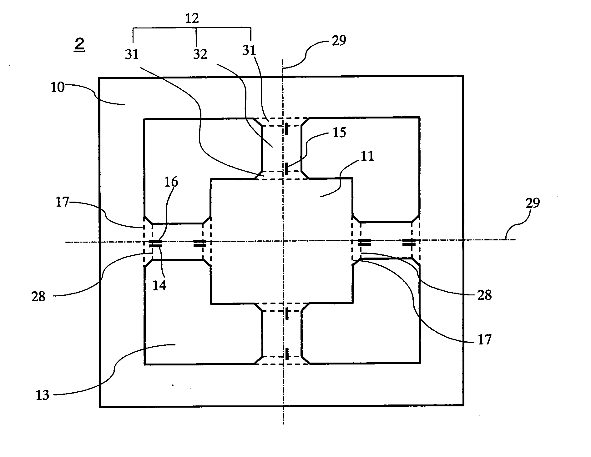
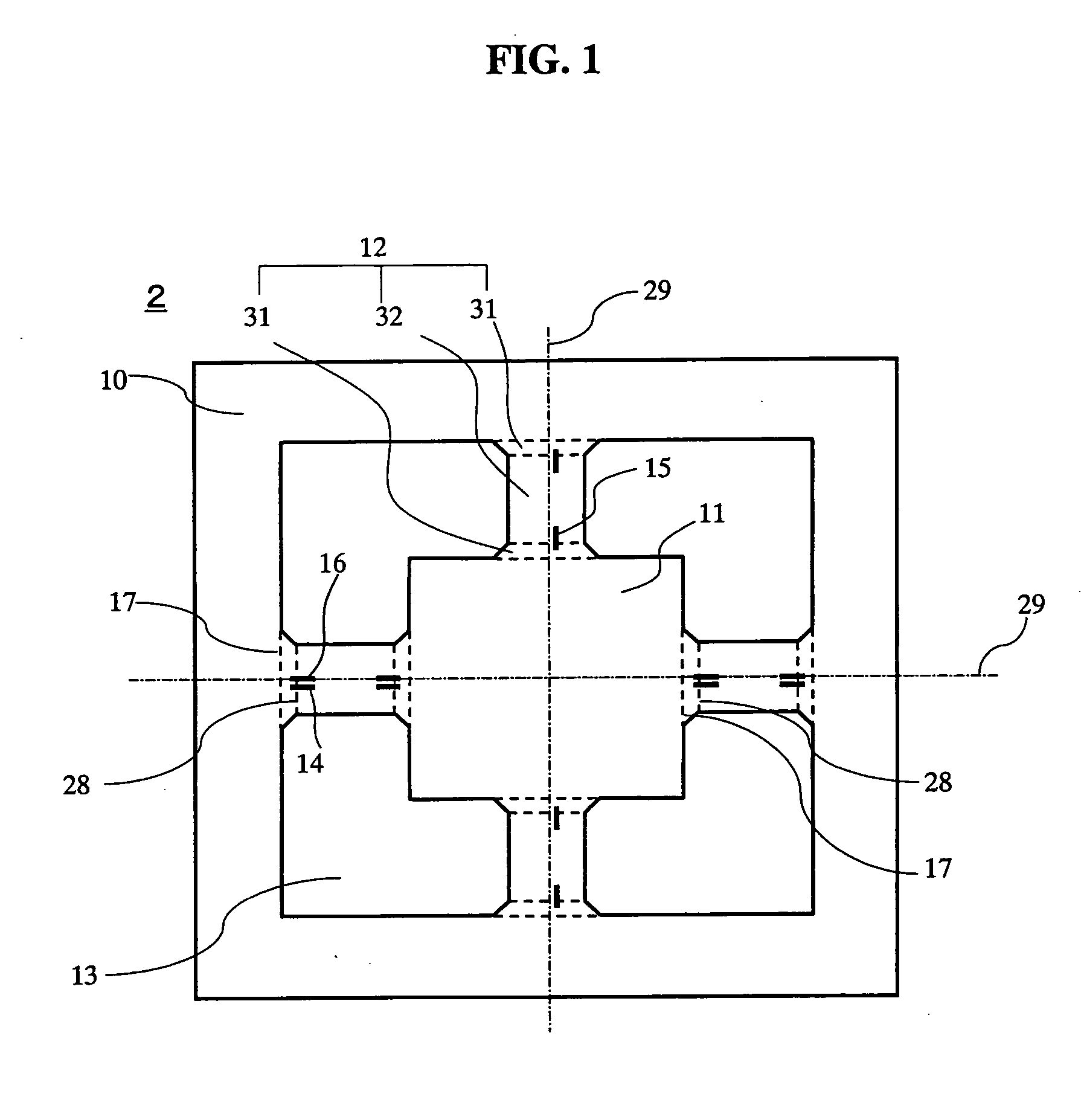
[0097]FIG. 5 is a graph showing a relationship of outputs to positions (L3) of maximum stress parts with a radius R of ridges of a flexible widening part as a parameter. FIG. 5 shows a case where the ridges of the flexible widening part 31 are ¼ circular arc. The flexible widening part, of which the ridges are a straight line or a noncircular arc, showed a similar tendency, so that the graph of the ¼ circular arc is shown here as a representative. In FIG. 5, radius R=0 μm means that the flexible winding part 31 does not exist, which shows a conventional sensor element only with a flexible parallel part 32 on a flexible arm. A maximum stress part in the conventional sensor element was at a connection end 17 of a flexible arm, at which L3=0 μm, and when a terminal of a piezo resistor 14, (15 or 16) was located at the connection end, an output of the piezo resistor was set to 100%. Positions (L3) indicating the maximum stress part were obtained while changing a radius R to 20 μm, 50 μm...

experiment 2

[0099] The following is a description of how to improve a shock resistance by providing a flexible widening part. FIG. 6 is a graph showing a relationship of shock resistances to lengths L1 of the flexible widening part, in which ridges of the flexible widening part are formed by a ¼ circular arc (R) with a radius R of 0 μm to 70 μm or a straight line with an angle of 45 degrees and in which distance (length L1 of the flexible widening part) between a connection end 17 of a flexible arm and a connection end 28 of a flexible parallel part is changed between 0 μm to 45 μm. Twenty acceleration sensors for each ridge were produced for shock resistance tests. A pendulum impact tester was used for the shock resistance test. An impacting time was set at 0.2 milliseconds. Accelerations of 1000 G to 5000 G were applied in steps of 100 G. Shock resistances may vary with direction, so that eighteen impacts, that is, six directions (a positive and a negative directions of X-axis, Y-axis and Z-a...

experiment 3

[0101]FIG. 7A is a graph showing a relationship of shock resistances (KG) and outputs (%) to W2 / W1, the ratio of the width W2 of the flexible parallel part 32 to the width W1 of the flexible widening part at the connection end 17 of the flexible arm. The width W2 of the flexible parallel part 32 in the flexible arm 12 was kept constant at 75 μm. As shown in the legends of FIG. 7B, the ridges of the flexible widening part were changed to ¼ circular arc with a radius R (indicated by ▪ and □), a straight line (indicated by ● and ∘), a mountain shape being steep in the vicinity of the connection end of the flexible arm (indicated by ▴ and Δ), and a bell shape changing sharply in shape in the vicinity of the connection end of a flexible parallel part (indicated by ♦ and ⋄). Twenty samples of the acceleration sensors with these ridges for each of the shapes were produced and evaluated by the same method as in the experiment 2 in the shock resistance test. Acceleration of 3 G was applied t...


PUM


Abstract

There is provided a semiconductor-type three-axis acceleration sensor having a high shock resistance, a small difference between outputs of piezo resistors of X-axis, Y-axis and Z-axis, a small size, high sensitivity and a high output. A flexible arm is composed of flexible widening parts and a flexible parallel part. The flexible widening part has a maximum stress part. The piezo resistors are arranged on an upper surface of the flexible arm so that a terminal of the piezo resistor is positioned at the maximum stress part. The Z-axis piezo resistors are positioned close to the width centerline of the flexible arm, while the X-axis and Y-axis piezo resistors are apart from the width centerline. Moreover, the Z-axis piezo resistors are shifted in the longitudinal direction of the flexible arm from the maximum stress part so as to reduce the output difference between the X-axis, Y-axis and Z-axis piezo resistors.

Description

TECHNICAL FIELD [0001] The present invention relates to a semiconductor-type three-axis acceleration sensor for use in automobiles, aircraft, consumer electronic products, gaming machines, robots, security systems and the like. BACKGROUND ART [0002] The structure of a piezo resistor-type three-axis acceleration sensor will be described below. FIG. 14 shows an exploded perspective view of a conventional acceleration sensor stated in Patent Document 1. In an acceleration sensor 1, a sensor element 2 is fixed to a protective case 3 with adhesive. A protective case lid 4 is fixed to the protective case 3 with adhesive. Sensor terminals 6 of the sensor element are connected to the case terminals 7 of the protective case by wires 5. The output of the sensor element 2 is delivered outward through external terminals 8. [0003] The following is a description of a sensor element used in a conventional piezo resistor-type three-axis acceleration sensor. Hereinafter, unless otherwise specified, ...

Claims


Application Information

Patent Timeline
Patent Type & Authority Applications(United States)
IPC IPC(8): G01P15/12G01P15/18
CPCG01P15/123G01P15/18G01P2015/084G01P2015/0842G01P15/08
Inventor TAKEYARI, TOKUHISAIKEDA, YOSHIO
Owner HITACHI METALS LTD
Why Eureka
Try Eureka