Semiconductor device and method for manufacturing thereof

a technology of semiconductor devices and semiconductors, applied in semiconductor devices, solid-state devices, basic electric elements, etc., can solve the problems of not being able to ensure the not being able to apply the technique to the die-bonding part that requires high reliability of the joint, and nothing being considered on the break of the joint suffering from thermal fatigue, etc., to achieve the effect of high melting poin

Inactive Publication Date: 2007-04-26
RENESAS ELECTRONICS CORP
View PDF3 Cites 26 Cited by
  • Summary
  • Abstract
  • Description
  • Claims
  • Application Information

AI Technical Summary

Benefits of technology

[0017] When the joint has been once made to have a high melting point by the above mentioned method, the joint can be maintained without being re-melted even by heating at 260° C. in the reflow soldering process.

Problems solved by technology

Therefore, it was not easy to apply the technique to the die-bonding part that requires high reliability of the joint in order to permit the joint to exhibit an important function as a heat dissipation passageway of the semiconductor element.
However, both in the patent documents 1 and 2, the joint is made by combining the bonding materials having a small difference of thermal expansion coefficients to one another, nothing was considered on the break of the joint suffering from thermal fatigue due to fragility as a result of making the joint to have a high melting point.
Consequently, a chip suffers from large load and cracks are generated in the chip to make it impossible to ensure reliability of the joint.
While it is possible to shorten the time necessary for forming the complete intermetallic compound by raising the bonding temperature, stress generated by cooling after bonding becomes larger to cause the cracks of the chip.

Method used


Image

  • Semiconductor device and method for manufacturing thereof
  • Semiconductor device and method for manufacturing thereof
  • Semiconductor device and method for manufacturing thereof

Examples


first embodiment

EXAMPLES 1 to 5

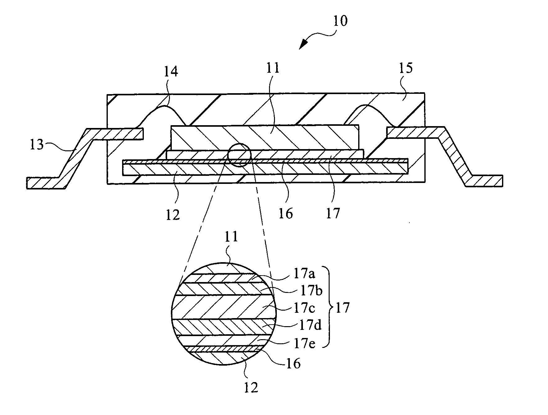
[0065]FIG. 3 shows a cross-section view of a power semiconductor device according to a first embodiment.

[0066] The semiconductor device 10 according to the first embodiment comprises a power semiconductor element 11, a frame 12 to which the power semiconductor element 11 is bonded, a lead 13 as an external terminal, a wire 14 for wire bonding between the electrode of the semiconductor element 11 and an inner lead of the lead 13, and an epoxy-based resin 15 for molding the semiconductor device with the resin with exposure of a portion that serves as an external terminal of the lead 13. The frame 12 has an Ni plating layer 16 on the surface thereof.

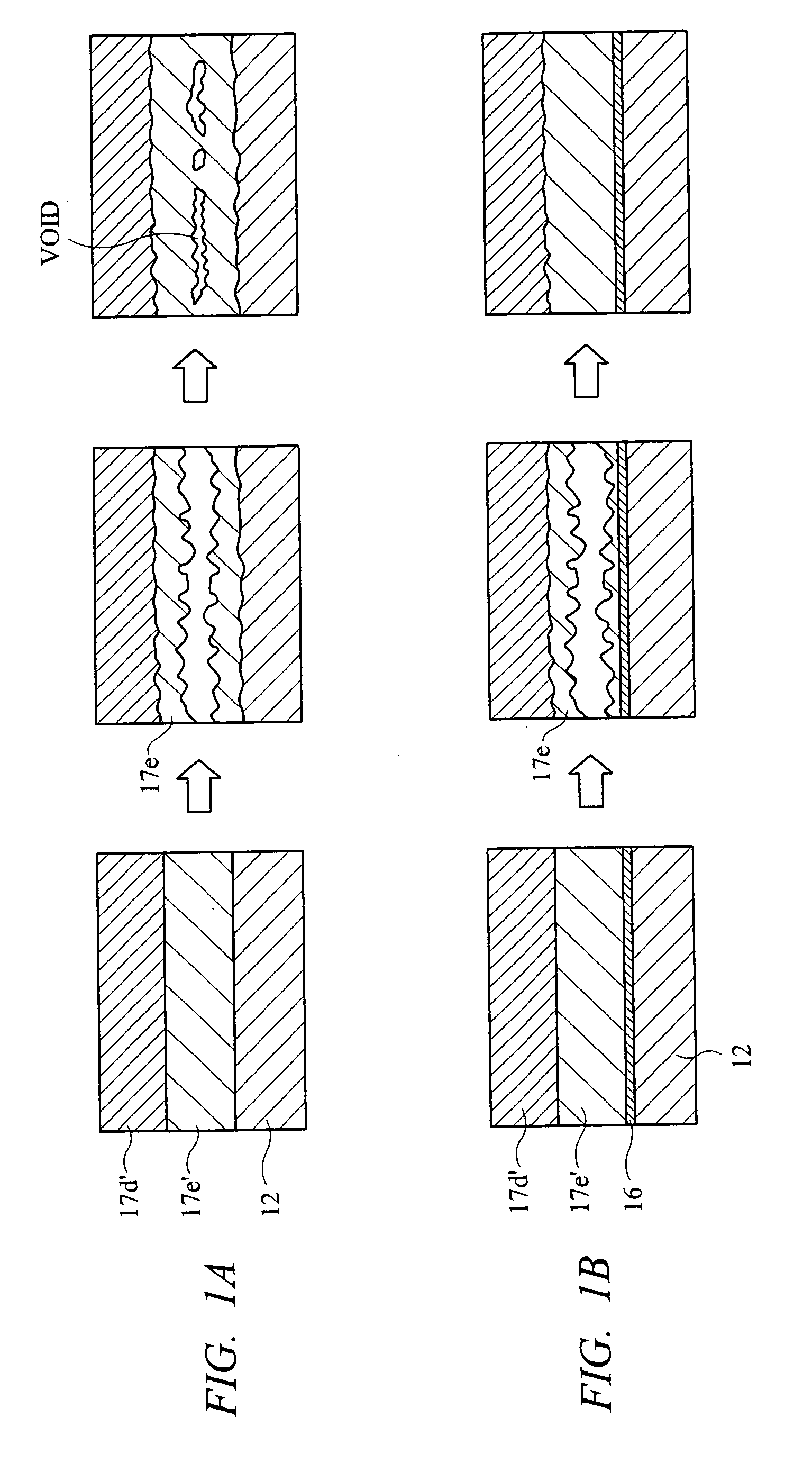
[0067] A joint 17 between the power semiconductor element 11 and the frame 12 having the Ni plating layer 16 is composed of a laminated structure comprising, from the power semiconductor element 11 side, an intermetallic compound layer 17e having a melting point of 260° C. or higher, a Cu layer 17b, a metal layer 17c havin...

second embodiment

EXAMPLES 6 to 10

[0079]FIG. 7 shows a cross-section view of a power semiconductor element according to a second embodiment of the present invention.

[0080] The power semiconductor device 30 according to the second embodiment of the present invention comprises a power semiconductor element 31, a drain frame 32a and a source-gate frame 32b to which the power semiconductor element 31 is bonded, and an epoxy-based resin 35 for molding the semiconductor device with the resin with exposure of the portions to serve as external terminals of the drain frame 32a and source-gate frame 32b. The surfaces of the drain frame 32a and source-gate frame 32b comprise Ni plated layers 36a and 36b, respectively.

[0081] In the power semiconductor device 30, joints 37a and 37b between the power semiconductor element 31 and drain frame 32a, and between the power semiconductor element 31 and the source-gate frame 32b, respectively, are composed of laminated structures each comprising, from the power semicon...

third embodiment

EXAMPLES 11 to 15

[0089]FIG. 8 shows a cross-section view of a power semiconductor device according to a third embodiment.

[0090] The power semiconductor device 40 according to the third embodiment of the present invention comprises power semiconductor elements 41a and 41b, a frame 42 to which the power semiconductor elements 41a and 41b are bonded, a terminal 43 that serves as an external terminal, wires 44 for wire bonding between respective electrodes of the power semiconductor elements 41a and 41b, and an epoxy-based resin 45 for molding the semiconductor device with the resin leaving the portions serving as the external terminals exposed. The frame 42 is plated by the Ni plating 46.

[0091] In the power semiconductor device 40, the joints 47a and 47b between the power semiconductor elements 41a and 41b and the frame 42 respectively, are composed of laminated structures comprising, from the power semiconductor elements 41a and 41b side, intermetallic compound layers having a melt...


PUM

PropertyMeasurementUnit
melting pointaaaaaaaaaa
melting pointsaaaaaaaaaa

Abstract

In a power semiconductor device, a joint between the power semiconductor element and frame plated with Ni is composed of a laminated structure comprising, from the power semiconductor element side, an intermetallic compound layer having a melting point of 260° C. or higher, a Cu layer, a metal layer having a melting point of 260° C. or higher, a Cu layer and an intermetallic layer having a melting point of 260° C. or higher. The structure of the joint buffers the stress generated by the secondary mounting and temperature cycle at the bond for the semiconductor element and the frame having a large difference in thermal expansion coefficient from each other.

Description

CROSS-REFERENCE TO RELATED APPLICATION [0001] The present application claims priority from Japanese Patent Application No. JP 2005-311047 filed on Oct. 26, 2005, the content of which is hereby incorporated by reference into this application. TECHNICAL FIELD OF THE INVENTION [0002] The present invention relates to a technology for manufacturing a semiconductor device, in particular to a technology effective for applying to a semiconductor device such as a power semiconductor device having joints comprising a lead-free intermetallic compound layer which contains no lead and a stress-buffering layer. BACKGROUND OF THE INVENTION [0003]FIG. 11 shows an example of the structure of a conventional power semiconductor device investigated by the inventors of the present invention as a premise. [0004] The conventional power semiconductor device 110 comprises a power semiconductor element 111 die-bonded on a frame 112 with a solder 117. After bonding the element to a lead 113 with a wire 114, t...

Claims


Application Information

Patent Timeline
Patent Type & Authority Applications(United States)
IPC IPC(8): C22F1/08
CPCC22F1/08H01L23/49513H01L23/49582H01L24/29H01L24/30H01L24/32H01L24/33H01L24/40H01L24/45H01L24/48H01L24/83H01L2224/32245H01L2224/32507H01L2224/45124H01L2224/45144H01L2224/48091H01L2224/48137H01L2224/48247H01L2224/73265H01L2224/83101H01L2224/83801H01L2924/01004H01L2924/01005H01L2924/01012H01L2924/01013H01L2924/01014H01L2924/01015H01L2924/01027H01L2924/01029H01L2924/0103H01L2924/01042H01L2924/01047H01L2924/01049H01L2924/0105H01L2924/01051H01L2924/01063H01L2924/01074H01L2924/01075H01L2924/01078H01L2924/01079H01L2924/01082H01L2924/01327H01L2924/10329H01L2224/2919H01L2224/83455H01L2924/01006H01L2924/01024H01L2924/01033H01L2924/014H01L2924/0665H01L2924/10253H01L2224/29101H01L2924/0132H01L2924/0133H01L2924/15747H01L2224/29109H01L2224/29111H01L2224/2908H01L2924/01028H01L2924/00014H01L2924/00012H01L2924/00H01L2924/3512H01L2924/351H01L2924/181H01L24/73H01L2224/84801H01L2224/37147H01L2224/37155H01L2224/3754H01L24/37H01L24/84H01L2224/2612H01L2224/73221
Inventor IKEDA, OSAMUOKAMOTO, MASAHIDEKAGII, HIDEMASAOKA, HIROINAKAMURA, HIROYUKI
Owner RENESAS ELECTRONICS CORP
Why Eureka
Try Eureka