Method for manufacturing a printed circuit board for electronic devices and an electronic device using the same

a printed circuit board and electronic device technology, applied in the direction of manufacturing tools, soldering devices, semiconductor/solid-state device details, etc., can solve the problems of limited application of sn-57bi-1ag solder, inability to provide secure connection reliability to solder connection parts, and inability to apply to a product with the part, so as to achieve the effect of reducing reliability and reducing connection reliability

Active Publication Date: 2007-04-26
FUJITSU LTD
View PDF7 Cites 22 Cited by
  • Summary
  • Abstract
  • Description
  • Claims
  • Application Information

AI Technical Summary

Benefits of technology

[0020] By the present invention, it is possible to obtain a soldering technology that secures the reliability of a whole electronic device, particularly a lead-free soldering technology that secures the reliability of a whole electronic device. To be more specific, it is possible to solve the problem of decrease of reliability in a whole electronic device that is caused by solder connection parts with a decreased connection reliability partly generated during the manufacture of a printed circuit board for the electronic device.

Problems solved by technology

, there is a problem that, if there is an electronic part with a low heat resistance, application to a product with the part is not possible due to the thermal damage incurred to the part.
However, the application of a Sn-57Bi-1Ag solder has been limited until now.
The reason is that there are some conventional electronic parts that have connection terminals with Sn-10Pb plating, and they cannot provide secure connection reliability to the solder connection parts due to a Bi—Pb—Sn alloy with a melting point not more than 100° C. generated at the solder connection parts during the connection by soldering.
% at the solder connection parts, caused by the transfer of Ag in the Sn-3Ag-0.5Cu composition during the connection by soldering, leading to a shorter fatigue life.
Thus, when assembling of a printed circuit board is carried out only with either one of the Sn-58Bi solder paste and Sn-57Bi-1Ag solder paste, there will be solder connection parts partly generated with decreased connection reliability, resulting in decrease in reliability of the whole device.

Method used


Image

  • Method for manufacturing a printed circuit board for electronic devices and an electronic device using the same
  • Method for manufacturing a printed circuit board for electronic devices and an electronic device using the same
  • Method for manufacturing a printed circuit board for electronic devices and an electronic device using the same

Examples


example 1

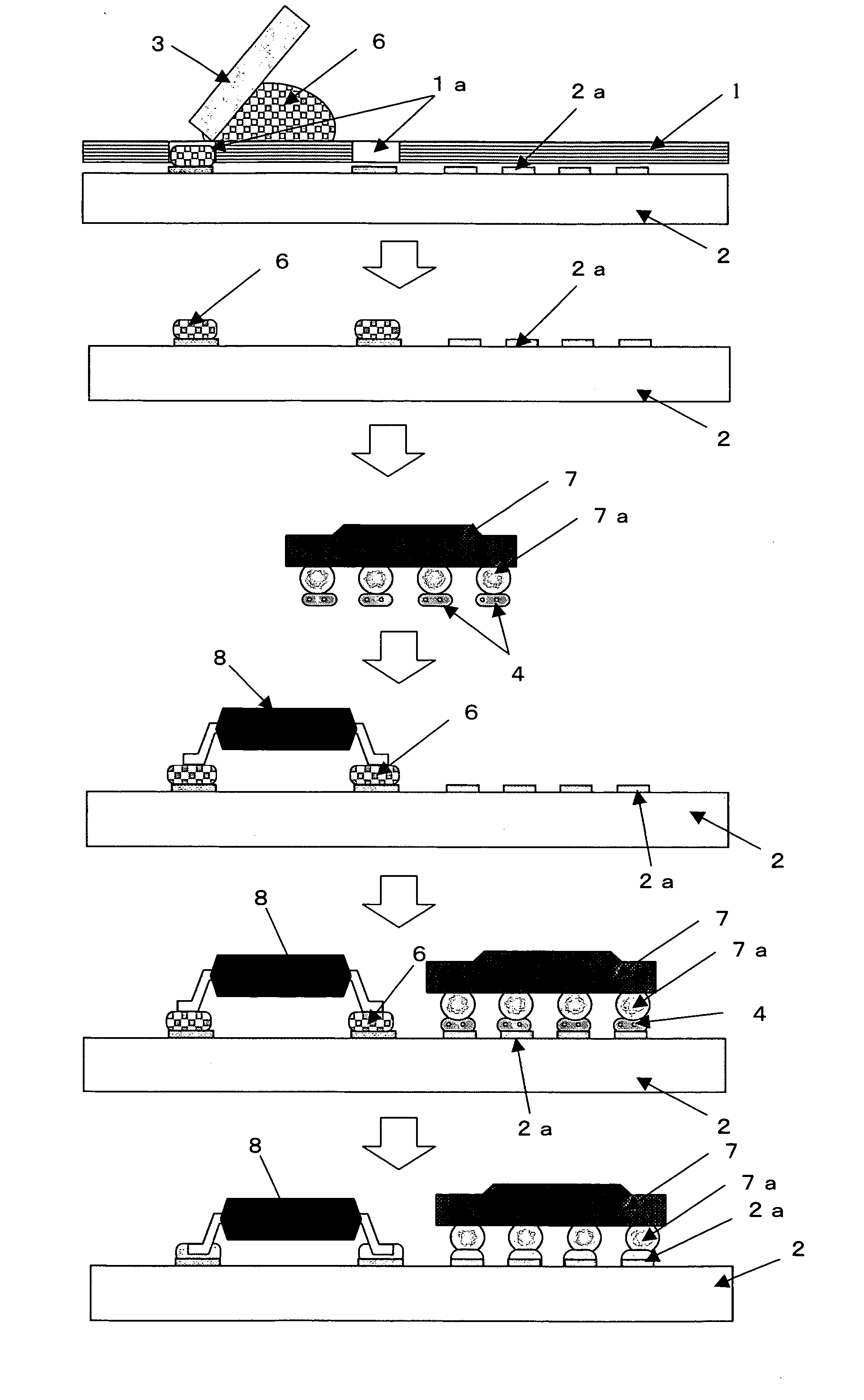
[0073] The steps shown in FIG. 1 were employed. The Sn-57Bi-1Ag solder paste 6 was printed on the substrate 2 through a metal mask 1 (0.15 mm thick) with through openings 1a formed corresponding to a 208-pin QFP part, and the QFP part 8 (208 pins) having lead connection terminals with Sn-3Bi plating was mounted on the solder paste.

[0074] Then, the Sn-58Bi solder paste 4 was supplied by the transfer method to be applied to the ball connection terminals of the BGA part (352 pins) 7 having ball connection terminals with a metal composition of Sn-3Ag-0.5Cu, the BGA part was mounted on specified substrate electrodes 2a, and the substrate was heated at 180° C. for the solder connection.

[0075] When the thermal cycle test under the temperature condition of −65° C. to 125° C. was carried out for the prepared printed circuit board samples, all the solder connection parts showed connection reliability values that corresponded to 10-year use.

example 2

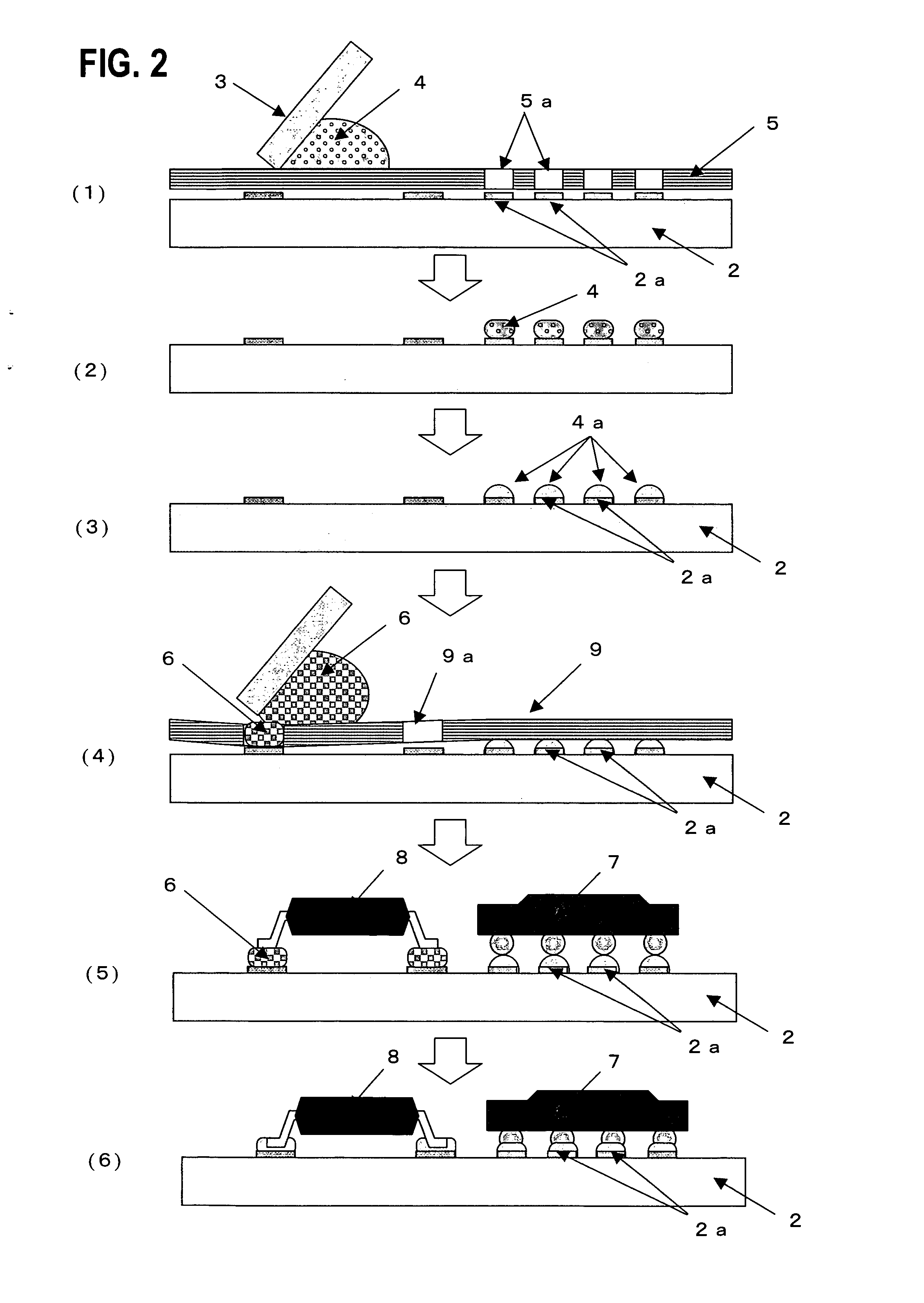
[0076] The steps shown in FIG. 2 were employed. The Sn-58Bi solder paste 4 was printed on the substrate 2 through a metal mask 5 (0.15 mm thick) with through openings 5a formed corresponding to a 352-pin BGA part. Then, the substrate was heated at 180° C. to form a presolder bump 4a on the substrate electrodes. Afterwards, the Sn-57Bi-1Ag solder paste 6 was printed on the substrate through a metal mask 9 (0.15 mm thick) with through openings 9a formed corresponding to a 208-pin QFP part.

[0077] Then, the BGA part (352 pins) 7 having ball connection terminals with a metal composition of Sn-3Ag-0.5Cu was mounted on the substrate electrodes on which the presolder bump 4a was placed, the QFP part (208 pins) 8 having lead connection terminals with Sn-3Bi plating was mounted on the electrodes on which the Sn-57Bi-1Ag solder paste 6 was printed, and then, the substrate was heated at 180° C. for the solder connection. A rosin-type liquid flux was applied to the Sn—Bi presolder bump 4a on th...

example 3

[0079] The steps shown in FIG. 3 were employed. The Sn-58Bi solder paste 4 was printed on the substrate 2 through a metal mask 10 (0.15 mm thick) with through openings 10a formed corresponding to a 352-pin BGA part. Then, the Sn-57Bi-1Ag solder paste 6 was printed on the substrate through a metal mask 11 (0.15 mm thick) with through openings 11a corresponding to a 208-pin QFP part, and with recessed parts 11b that did not pass through the metal mask formed by half etching on the locations corresponding to the Sn-58Bi paste-printed parts.

[0080] Then, the BGA part (352 pins) 7 having ball connection terminals with a metal composition of Sn-3Ag-0.5Cu was mounted on the electrodes on which the Sn-58Bi solder paste 4 had been printed, the QFP part (208 pins) 8 having lead connection terminals with Sn-3Bi plating was mounted on the electrodes on which the Sn-57Bi-1Ag solder paste 6 was printed, and the substrate was heated at 180° C. for the solder connection.

[0081] When the thermal cyc...


PUM

PropertyMeasurementUnit
melting pointaaaaaaaaaa
temperatureaaaaaaaaaa

Abstract

A soldering technology, particularly a lead-free soldering technology, that can secure the reliability of a whole electronic device is provided. In a method for manufacturing a printed circuit board for electronic devices with a substrate to which a plurality of electronic parts having connection terminals with different metal compositions are connected by soldering, a plurality of solder pastes comprising solder components with different compositions are used, and when the electronic parts are connected by soldering to the substrate, a solder paste having a solder component with a different composition is used for each of the metal compositions for the connection terminals of the electronic parts.

Description

CROSS-REFERENCE TO RELATED APPLICATIONS [0001] This application is based upon and claims the benefit of priority from the prior Japanese Patent Application No. 2005-310202, filed on Oct. 25, 2005, the entire contents of which are incorporated herein by reference. BACKGROUND OF THE INVENTION [0002] 1. Field of the Invention [0003] The present invention relates to a new method for manufacturing a printed circuit board for electronic devices and an electronic device for which the printed circuit board is used. [0004] 2. Description of the Related Art [0005] The surface mounting technology is known as a method for manufacturing a printed circuit board for electronic devices. In the surface mounting technology, electronic parts can be mounted densely, and therefore, it provides a merit of realizing miniaturization and weight-reduction of electronic devices. [0006] According to a printed circuit board manufacturing (assembling) process by the surface mounting technology, a solder paste is...

Claims


Application Information

Patent Timeline
Patent Type & Authority Applications(United States)
IPC IPC(8): B23K31/02B23K35/24
CPCB23K3/0623B23K2201/40H01L2924/15311H05K3/3421H05K3/3436H05K3/3463H05K3/3484H05K2201/10689H05K2201/10734H05K2201/10984H05K2203/043H05K2203/1476B23K2101/40H05K3/3485
Inventor OCHIAI, MASAYUKIUCHIDA, HIROKIAKAMATSU, TOSHIYA
Owner FUJITSU LTD
Why Eureka
Try Eureka