Nitride semiconductor light emitting device

a light-emitting device and nitride technology, applied in semiconductor devices, semiconductor lasers, lasers, etc., can solve the problems of reducing internal quantum efficiency, increasing the distance between electron wave function and hole wave function, and affecting the efficiency so as to improve the internal quantum efficiency and luminance of nitride semiconductor light-emitting devices, reduce the effect of strain in the active layer

Active Publication Date: 2007-04-26
SAMSUNG ELECTRONICS CO LTD
View PDF9 Cites 26 Cited by
  • Summary
  • Abstract
  • Description
  • Claims
  • Application Information

AI Technical Summary

Benefits of technology

[0010] The present invention has been made to solve the foregoing problems of the prior art and therefore an object of certain embodiments of the present invention is to provide a high quality nitride semiconductor light emitting device which has high internal quantum efficiency and brightness and uniform energy level in a quantum well.
[0011] According to an aspect of the invention for realizing the object, the invention provides a nitride semiconductor light emitting device. The nitride semiconductor light emitting device includes an n-nitride semiconductor layer; an active layer of multi-quantum well structure formed on the n-nitride semiconductor layer, and having a plurality of quantum well layers and a plurality of quantum barrier layers; and a p-nitride semiconductor layer formed on the active layer. One of the quantum well layers adjacent to the n-nitride semiconductor layer has an energy band gap greater than that of another one of the quantum well layers adjacent to the p-nitride semiconductor layer. With the quantum well layer adjacent to the n-nitride semiconductor layer having a greater energy band gap, it is possible to reduce strain owing to the lattice mismatch between the n-nitride semiconductor layer and the active layer without having an effect on the wavelength of emitted light.
[0014] According to a preferred embodiment of the invention, each of the quantum well layers has a greater energy band gap with the quantum well layer being more adjacent to the n-nitride semiconductor layer. With the quantum well layer adjacent to the n-nitride semiconductor layer having a greater energy band gap, it is possible to reduce strain in the active layer. Such a band gap structure can be realized by the In content change of the quantum well layer. That is, by making the quantum well layer have a greater In content when more adjacent to the n-nitride semiconductor layer, the band gap of the quantum well layer can be made greater when the quantum well layer is more adjacent to the n-nitride semiconductor layer.
[0016] According to this invention, strain occurring in the active layer can be alleviated by adjusting the band gaps of the quantum well layers. This as a result raises internal quantum efficiency and luminance of the nitride semiconductor light emitting device. Furthermore, potential barrier lowered in the vicinity of the n-nitride semiconductor layer causes increase in electron injection efficiency without wavelength change of emitted light. This can obtain effects of improved luminance and decreased operating (forward) voltage. Furthermore, the quantum well layer having uniform quantum level can suppress creation of blue shift.

Problems solved by technology

Such lattice mismatch causes a considerable amount of strain in the active layer.
The strain in turn generates a piezoelectric field in the active layer, which increases the distance between electron wave function and hole wave function but lowers internal quantum efficiency.
In addition, the strain in the active layer acts to degrade the uniformity of energy level in each quantum well.

Method used


Image

  • Nitride semiconductor light emitting device
  • Nitride semiconductor light emitting device
  • Nitride semiconductor light emitting device

Examples


Embodiment Construction

[0022] Preferred embodiments of the present invention will now be described in detail with reference to the accompanying drawings. The invention may however be embodied in many different forms and should not be construed as limited to the embodiments set forth herein. Rather, these embodiments are provided so that this disclosure will be thorough and complete, and will fully convey the scope of the invention to those skilled in the art.

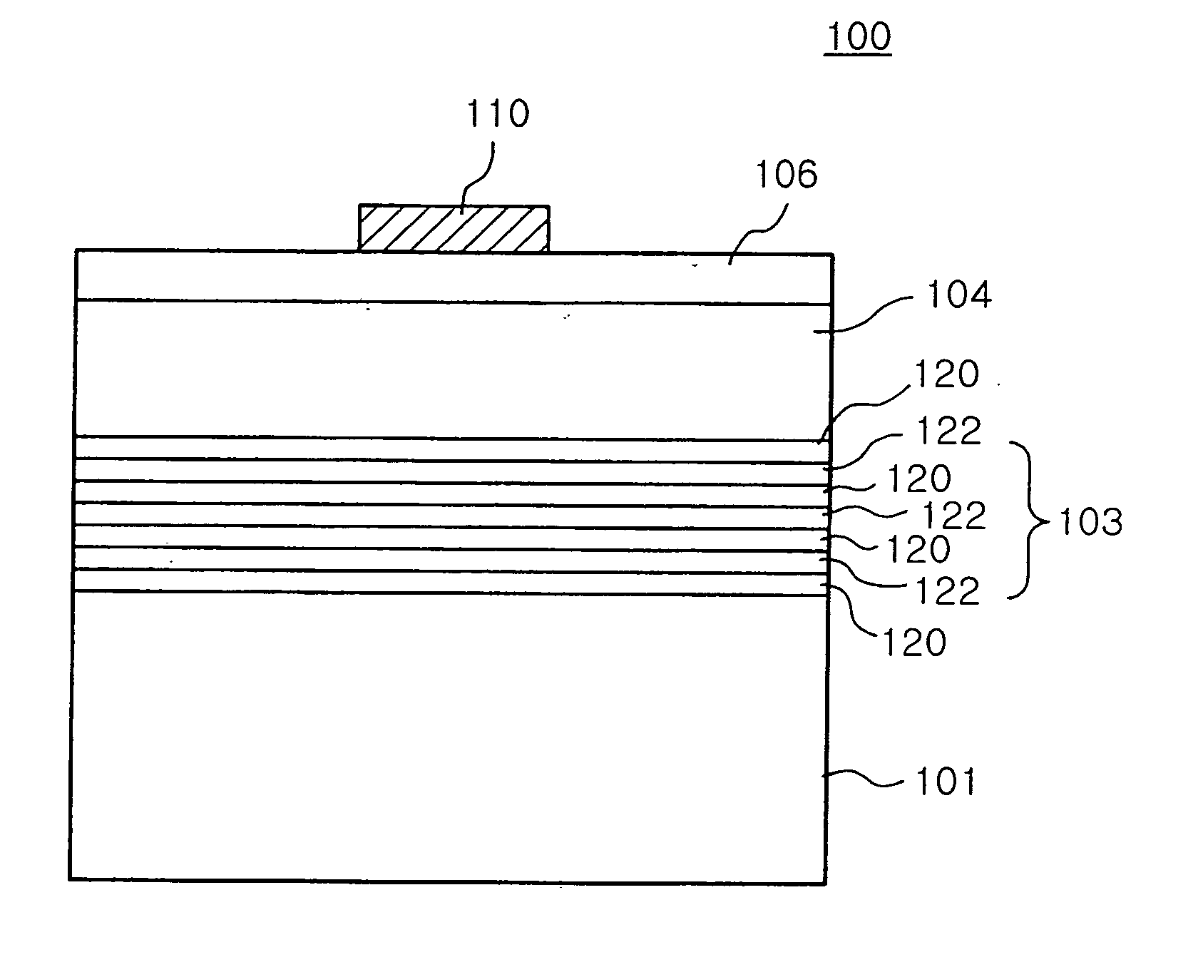
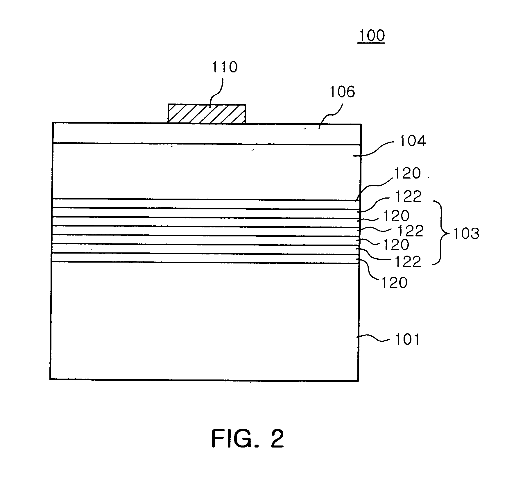
[0023]FIG. 2 is a cross-sectional view illustrating a nitride semiconductor light emitting device 100 according to an embodiment of the invention. Referring to FIG. 2, the nitride semiconductor light emitting device 100 includes an n-nitride semiconductor layer 101, and includes an active layer 103 and a p-nitride semiconductor layer 104 sequentially stacked on the n-nitride layer 101. On the p-nitride semiconductor layer 104, formed are a p-contact layer 106 and a p-electrode 110. The light emitting device 100 may be of a lateral structure or a vert...


PUM


Abstract

A nitride semiconductor light emitting device has high internal quantum efficiency but low operating voltage. The nitride semiconductor light emitting device includes an n-nitride semiconductor layer; an active layer of multi-quantum well structure formed on the n-nitride semiconductor layer, and having a plurality of quantum well layers and a plurality of quantum barrier layers; and a p-nitride semiconductor layer formed on the active layer. One of the quantum well layers adjacent to the n-nitride semiconductor layer has an energy band gap greater than that of another one of the quantum well layers adjacent to the p-nitride semiconductor layer.

Description

CLAIM OF PRIORITY [0001] This application claims the benefit of Korean Patent Application No. 2005-100782 filed on Oct. 25, 2005, in the Korean Intellectual Property Office, the disclosure of which is incorporated herein by reference. BACKGROUND OF THE INVENTION [0002] 1. Field of the Invention [0003] The present invention relates to a nitride semiconductor light emitting device, and more particularly, to a high quality nitride semiconductor light emitting device having high internal quantum efficiency but low operating voltage. [0004] 2. Description of the Related Art [0005] To date, Light Emitting Diodes (LEDs) or Laser Diodes (LDs) based on group III-V nitride semiconductor (hereinafter will be referred to as “nitride semiconductor” in short) are often used in light emitting devices for generating a blue or green wavelength of light, and applied as light sources of various products such as an electronic display board and lighting equipment. Such nitride semiconductor is made of a...

Claims


Application Information

Patent Timeline
Patent Type & Authority Applications(United States)
IPC IPC(8): H01L31/00H01L33/06H01L33/32
CPCB82Y20/00H01L33/06H01L33/32H01S5/34333
Inventor LEE, DONG YULKANG, SANG WONSONG, KEUN MANKIM, JE WONHONG, SANG SU
Owner SAMSUNG ELECTRONICS CO LTD
Why Eureka
Try Eureka