CMOS image sensor and manufacturing method thereof

a technology of image sensor and manufacturing method, which is applied in the direction of diodes, radiation control devices, semiconductor devices, etc., can solve the problems of noise from dispersed lights, and achieve the effect of preventing or substantially reducing the dispersed light incident and improving the performance of the devi

Inactive Publication Date: 2007-04-26
DONGBU ELECTRONICS CO LTD
View PDF5 Cites 15 Cited by
  • Summary
  • Abstract
  • Description
  • Claims
  • Application Information

AI Technical Summary

Benefits of technology

[0015] An object of many embodiments of the present invention is to provide a CMOS image sensor and a method for manufacturing the same, which can prevent or substantially reduce a dispersion of light being incident to a photo diode through a micro lens.
[0016] Another object of many embodiments of the present invention is to provide a CMOS image sensor capable of improving a performance of a device by securing uniformity of incident light.

Problems solved by technology

Moreover, noise from the dispersed lights occurs in an adjacent photo diode.

Method used


Image

  • CMOS image sensor and manufacturing method thereof
  • CMOS image sensor and manufacturing method thereof
  • CMOS image sensor and manufacturing method thereof

Examples


Embodiment Construction

[0025] Reference will now be made in detail to the preferred embodiments of the present invention, examples of which are illustrated in the accompanying drawings. Wherever possible, the same reference numbers will be used throughout the drawings to refer to the same or like parts.

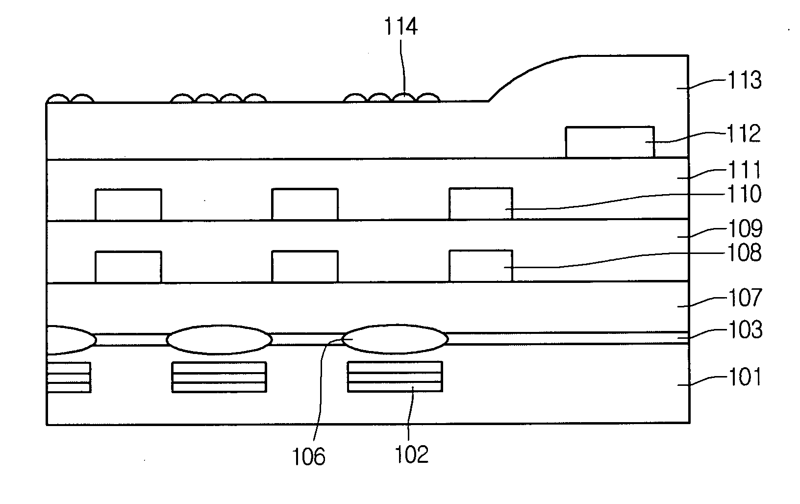
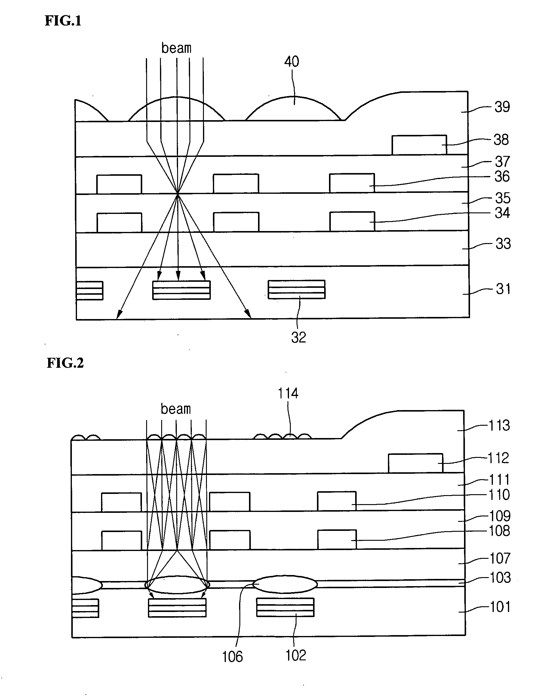
[0026]FIG. 2 is a cross-sectional view of a CMOS image sensor according to an embodiment of the present invention.

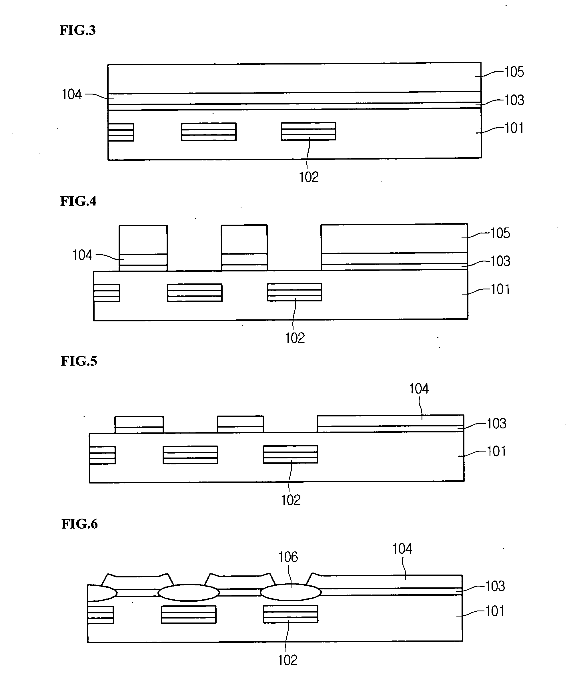
[0027] With reference to FIG. 2, a photo diode 102 can be formed in a substrate 101, and an oxide film 103 can be formed on the semiconductor substrate 101 including photodiode 102.

[0028] In one embodiment, the photo diode 102 can be formed to sense red (R), green (G), and blue (B) signals according to a wavelength of incident light.

[0029] A first micro lens 106 can be formed above the photo diode 102. The first micro lens 106 can be formed interposed in a part of the oxide film 103. That is, the first micro lens 106 can be formed to penetrate part of the oxide film.

[0030] A first inter-lay...


PUM


Abstract

A CMOS image sensor and a method for manufacturing the same are provided. The CMOS image sensor includes: a photo diode formed in a semiconductor substrate for generating an optical signal from incident light; a first micro lens formed on the semiconductor substrate above the photo diode; a plurality of inter-layer dielectrics and metal wires formed on the semiconductor substrate having the first micro lens; a planarization layer formed above the plurality of inter-layer dielectrics metal wires; and a second micro lens formed on the planarization layer. In one embodiment, the second micro lens incorporates a fly-eye pattern.

Description

RELATED APPLICATION(S) [0001] This application claims the benefit, under 35 U.S.C. §119(e), of Korean Patent Application Number 10-2005-0100201 filed Oct. 24, 2005, which is incorporated herein by reference in its entirety. FIELD OF THE INVENTION [0002] The present invention relates to an image sensor. BACKGROUND OF THE INVENTION [0003] In general, image sensors are semiconductor devices that transform an optical image to electrical signals. The CMOS image sensor is a device that employs a switching mode to sequentially detect an output of each unit pixel by means of MOS transistors using control circuits and signal-processing circuits. Each unit pixel incorporates a photodiode. [0004] In making such various image sensors, efforts are being made to improve the photosensitivity of the image sensor. [0005] For example, the CMOS image sensor is composed of a photo diode for sensing light and a CMOS logic circuit for processing the sensed light into electric signals. For better photosen...

Claims


Application Information

Patent Timeline
Patent Type & Authority Applications(United States)
IPC IPC(8): H01L31/113H01L31/06H01L31/062H01L21/8242
CPCH01L27/14625H01L27/14627H01L27/14632H01L27/14636H01L27/14643H01L27/14647H01L27/14687H01L27/14689H01L27/146
Inventor LEE, JUN SEOK
Owner DONGBU ELECTRONICS CO LTD
Why Eureka
Try Eureka