Eureka AIR delivers breakthrough ideas for toughest innovation challenges, trusted by R&D personnel around the world.

Light source structure

Inactive Publication Date: 2007-05-03
SUTECH TRADING LIMITED
View PDF5 Cites 21 Cited by
  • Summary
  • Abstract
  • Description
  • Claims
  • Application Information

AI Technical Summary

Benefits of technology

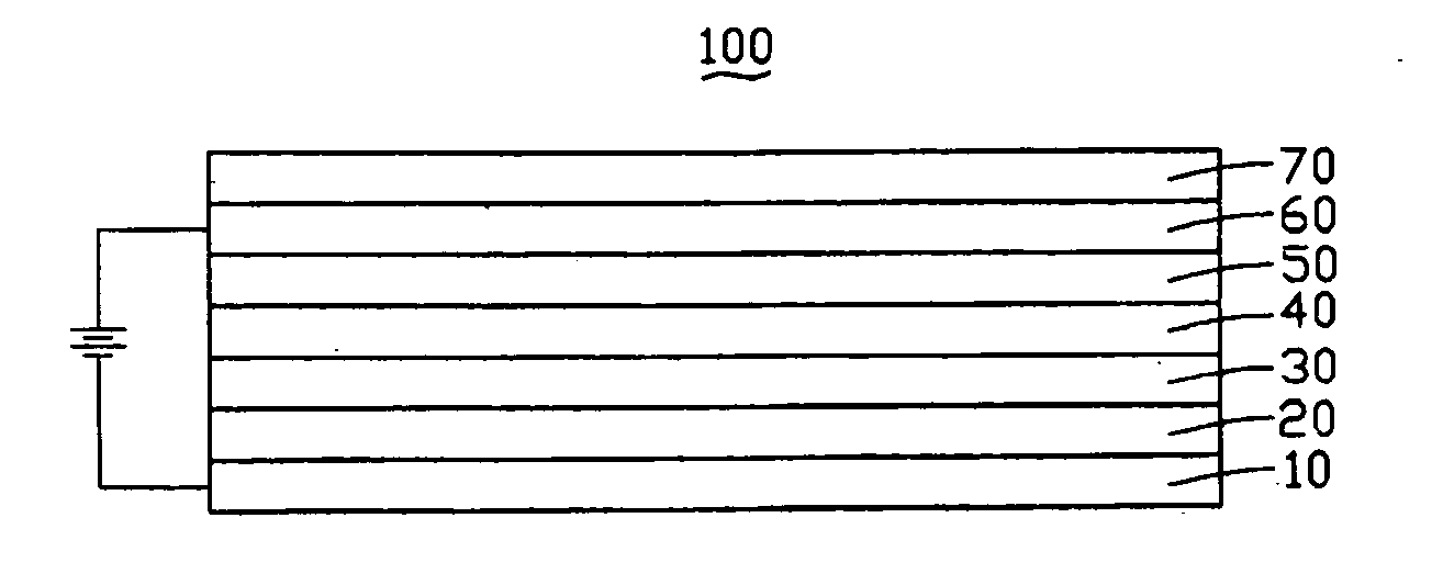
[0006] According to the present light source, a light source structure is provided. The light source structure is adapted for providing backlights to an LCD panel. The light source structure includes a cathode layer, a semiconductor layer, a dielectric layer, a nano-metallic compound (NMC) layer, and an anode layer. The semiconductor layer is disposed on the cathode layer, for emitting electrons when excited by an electric field. The dielectric layer is disposed on the semiconductor layer. The nano-metallic compound (NMC) layer is disposed on the dielectric layer. The NMC layer includes a plurality of NMC atom groups and is adapted for emitting lights when bombarded by electrons. The anode layer is disposed on the NMC layer, for providing an electric field, functionally associating with the cathode layer. The light source structure may further include a fluorescent layer disposed between the NMC layer and the anode layer, and / or a protection layer disposed on the anode layer for protecting the light source structure from being damaged and / or contaminated.
[0007] An advantage of the light source structure is that the light source structure is solid and not easy to be broken, and has a relatively long operating lifetime.
[0008] Another advantage of the light source structure is that the light source structure has higher light emitting efficiency.

Problems solved by technology

However, CCFLs are vulnerable and have shorter operating lifetimes. As such, LEDs using CCFLs usually have unsatisfactory light emitting efficiencies.

Method used


Image

  • Light source structure
  • Light source structure
  • Light source structure

Examples


Embodiment Construction

[0015] Reference will now be made to the drawings to describe the preferred embodiments of the present light source structure in detail.

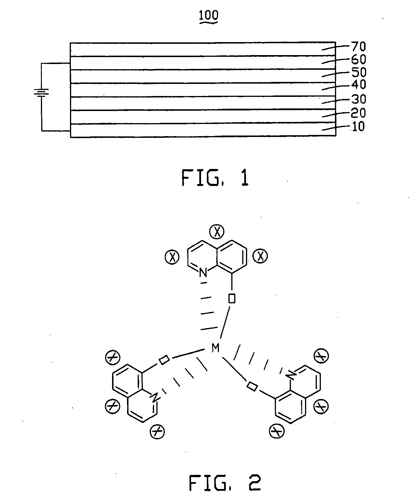
[0016] Referring now to the drawings, and more particularly to FIG. 1, there is shown a light source structure 100. The light source structure 100 includes a cathode layer 10, a semiconductor layer 20, a dielectric layer 30, a nano-metallic compound (NMC) layer 40 including a plurality of NMC atom groups, and an anode layer 60, all of the layers being stacked one on another in sequence from bottom to top. The cathode layer 10 is made of Cu, Ag, or Au. The semiconductor layer 20 is adapted for emitting electrons when applied with an electric field. The dielectric layer 30 is preferably a SiNx ceramic layer. The metallic compound layer 40 is composed of NMC particles being adapted for emitting lights of the range from 400 nm to 700 nm.

[0017] In operation, an electric field is applied between the cathode layer 10 and the anode layer 60. The applied e...


PUM


Abstract

A light source structure (100) for providing backlights to an LCD panel is provided. The light source structure includes a cathode layer (10), a semiconductor layer (20) disposed on the cathode layer, for emitting electrons when applied with electric field, a dielectric layer (30), disposed on the semiconductor layer a nano-metallic compound (NMC) layer (40), disposed on the dielectric layer, comprising a plurality of NMC atom groups, the NMC layer being adapted for emitting lights when bombarded by electrons, and an anode layer (60), disposed on the NMC layer, for providing an electric field together with the cathode layer. The light source structure may further include a fluorescent layer (50) disposed between the NMC layer and the anode layer, and / or a protection layer (70) disposed on the anode layer for protecting the light source structure from being damaged and / or contaminated.

Description

BACKGROUND [0001] 1. Technical Field [0002] The present invention relates to a light source structure and, particularly, to a light source structure having a nano-metallic compound (NMC) layer for enhancing a light emitting efficiency of an LCD device. [0003] 2. RELATED ARTS [0004] Liquid crystal displays (LCDs) themselves do not emit lights. In order to display images, an LCD panel usually needs a backlight module. A backlight module generally includes a light source and a light guide plate. Conventional light sources for LCDs are often cold cathode fluorescent lamps (CCFLs) or light emitting diodes (LEDs). [0005] However, CCFLs are vulnerable and have shorter operating lifetimes. As such, LEDs using CCFLs usually have unsatisfactory light emitting efficiencies. Therefore, new light sources are highly demanded for LCD panels. SUMMARY [0006] According to the present light source, a light source structure is provided. The light source structure is adapted for providing backlights to ...

Claims


Application Information

Patent Timeline
IPC IPC(8): H01L33/00
CPCC09K11/565C09K11/62C09K11/883H01J1/63H05B33/14
Inventor CHEN, GA-LANE
Owner SUTECH TRADING LIMITED
Why Eureka
Eureka Blog
Learn More