
Structure and manufacturing method of power semiconductor with twin metal and ceramic plates

a technology of power semiconductor and ceramic plate, which is applied in the direction of semiconductor devices, semiconductor/solid-state device details, electrical apparatus, etc., can solve the problems of reducing the life of use of power semiconductor, and achieve the reduction of heat storage and sealing amount, fast transmission, and heat conductivity

Inactive Publication Date: 2007-05-03
HUANG WEN PING
View PDF1 Cites 1 Cited by
  • Summary
  • Abstract
  • Description
  • Claims
  • Application Information

AI Technical Summary

Benefits of technology

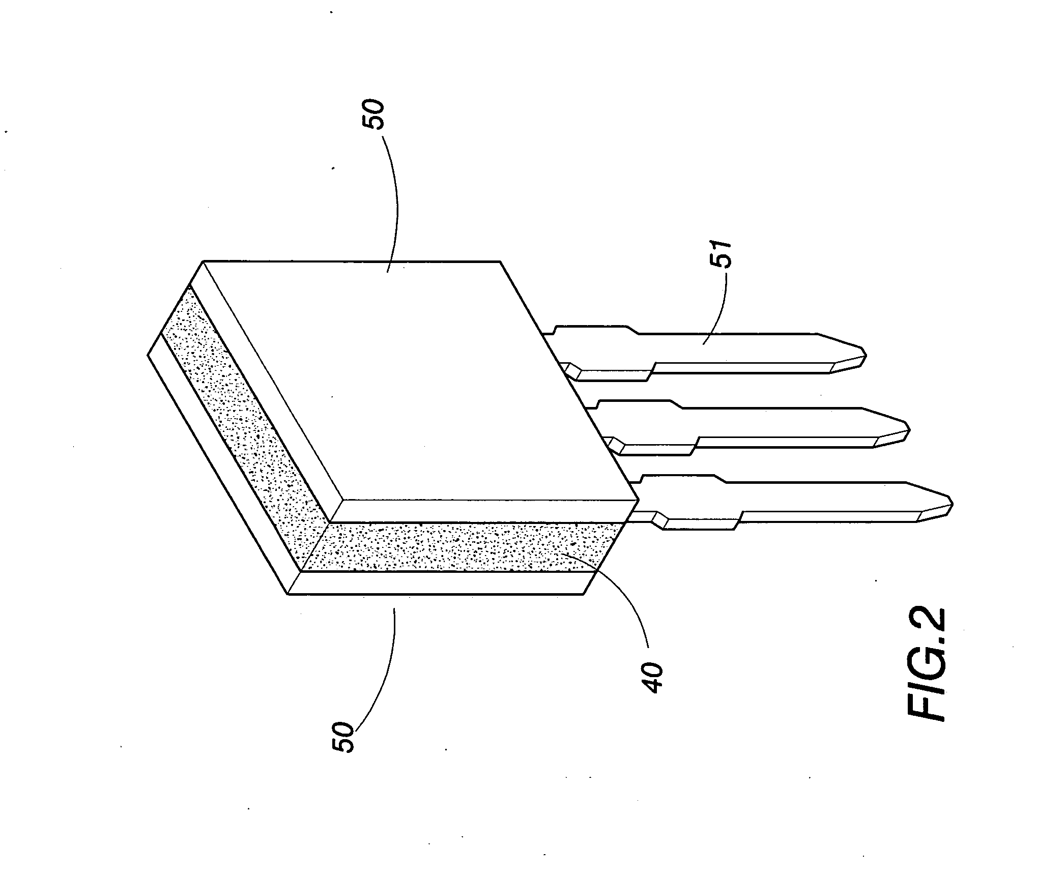
[0012] The object of the present invention is: to make the heat generated in operation of the silicon chip (when electric current passes through the two metallic base plates) be fast transmitted to the two metallic base plates through the ceramic base plate by having the surfaces of the ceramic base plate metallized and the two lateral sides of the ceramic base plate combined with the two metallic base plates all by a high temperature sintering technique. In comparison with the structure of the conventional power semiconductor, the heat conductivity of the ceramic base plate of the present invention is better than that of the epoxy resin layer, the amount of the heat stored and sealed can be largely reduced, and the area of heat sinking of the two metallic base plates can be increased at least to twofold of that of the conventional power semiconductor, thus the power semiconductor with twin metal plates and a ceramic plate sintered together of the present invention can be used for a long period in a high temperature environment, and thereby the life of use of the power semiconductor can be increased.
[0013] Another object of the present invention is to render the process of manufacturing simplified and the efficiency of automation production increased by having the ceramic shaped firstly and then combined with the metallic heat conducting plates by a high temperature sintering technique (in this way, the process of manufacturing can be different from the conventional one and needs no complicated process and equipment for plastic sealing).

Problems solved by technology

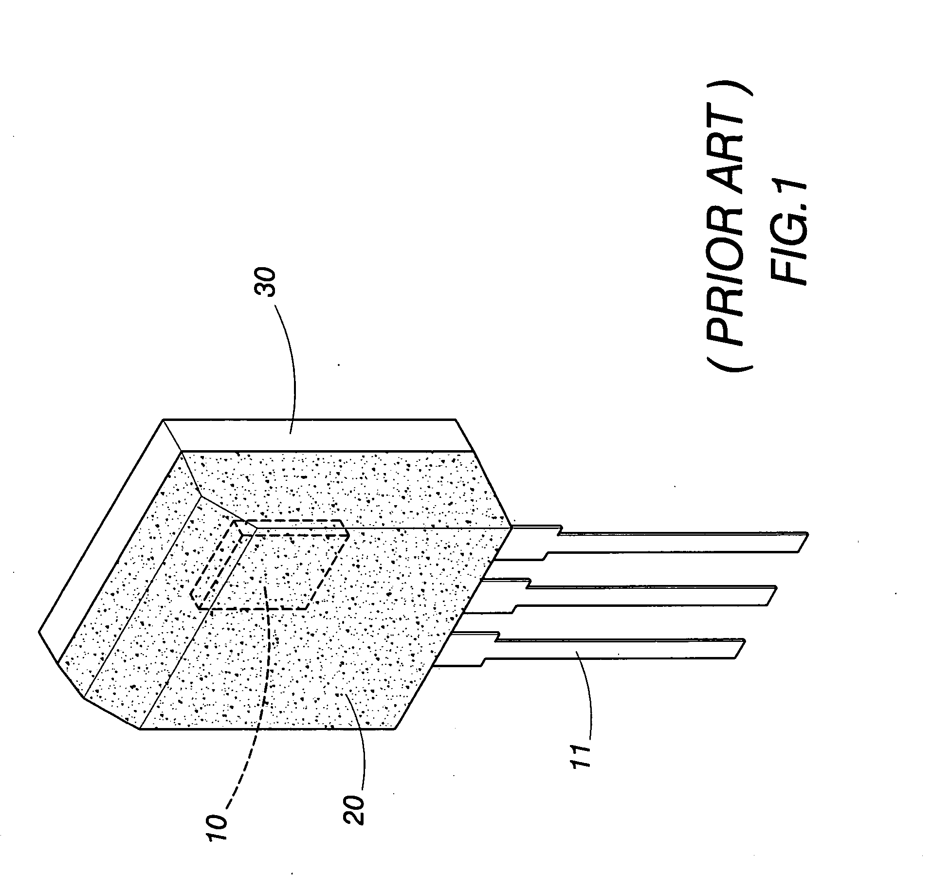
However, when the heat generated in operation of the power semiconductor is transmitted to the outer epoxy resin layer 20, by virtue that the epoxy resin layer 20 has inferior heat conductivity, after using for a long period, the epoxy resin layer 20 will absorb heat energy and store / seal the heat energy which is hard to dissipate in the power semiconductor; this is subjected to inducing overheating of the power semiconductor that renders the latter unable to operate normally, and thereby reduces the life of use of the power semiconductor.

Method used


Image

  • Structure and manufacturing method of power semiconductor with twin metal and ceramic plates
  • Structure and manufacturing method of power semiconductor with twin metal and ceramic plates
  • Structure and manufacturing method of power semiconductor with twin metal and ceramic plates

Examples


Embodiment Construction

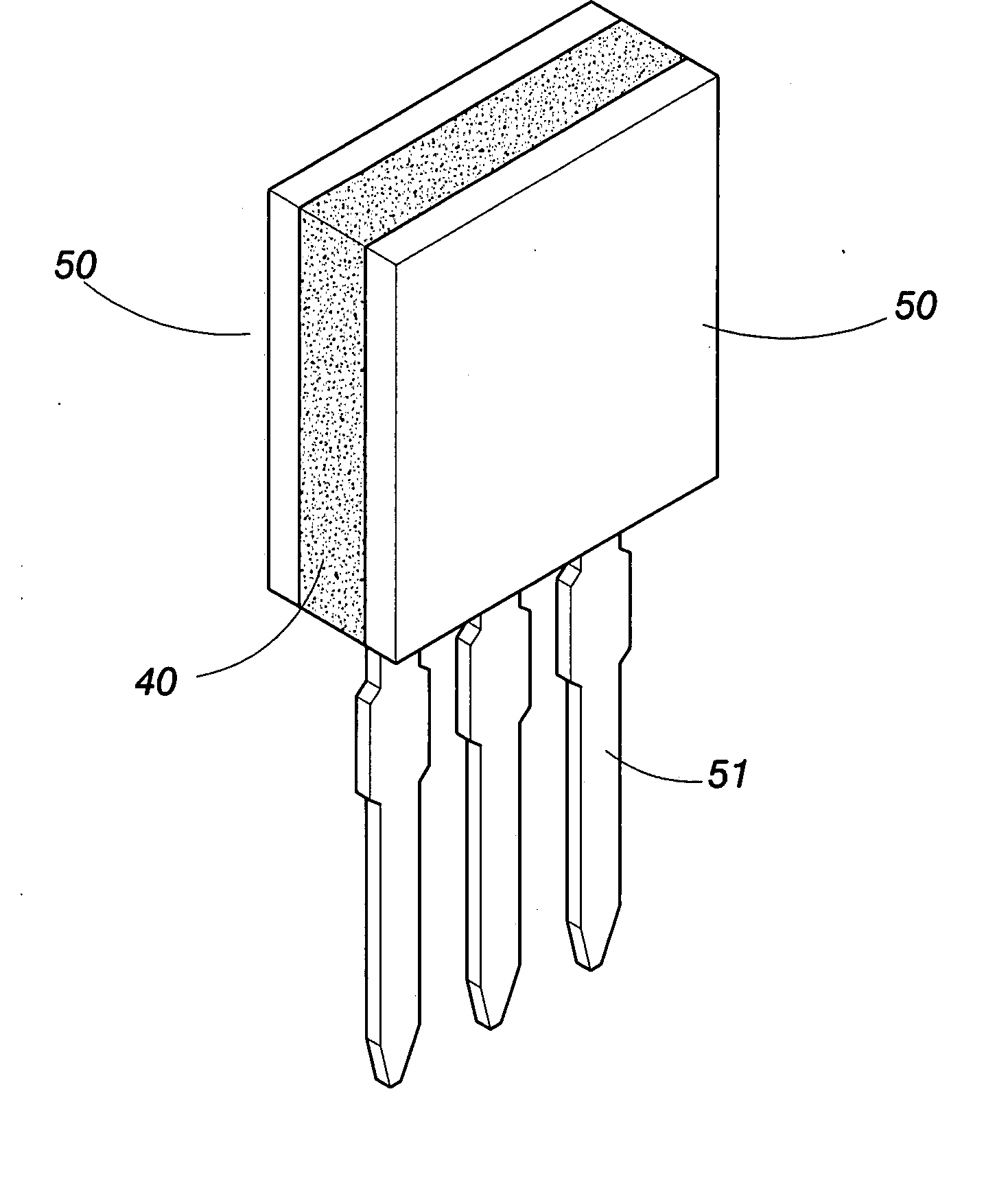
[0020] Referring to FIGS. 2-4, in “the structure and the method of manufacturing a power semiconductor with twin metal plates and a ceramic plate” of the present invention, the power semiconductor mainly is composed of a silicon chip 10, a ceramic base plate 40 and two metallic base plates 50, wherein the ceramic base plate 40 is provided with a receiving groove 41 to receive the silicon chip 10; the two lateral sides of the ceramic base plate 40 are combined with the two metallic base plates 50 by a high temperature sintering technique, thereby the silicon chip 10 is contacted and electrically communicated with the two metallic base plates 50, and the two metallic base plates 50 have connecting pins 51 extending outwards therefrom, and the structure of the power semiconductor with the twin metal plates and the ceramic plate thus is formed.

[0021] In using the power semiconductor with the twin metal plates and the ceramic plate, because that heat can be generated when electric curre...


PUM

PropertyMeasurementUnit
temperatureaaaaaaaaaa

Abstract

A designing for a power semiconductor, and especially to a structure of a power semiconductor formed by using the basic materials including two metal plates and a ceramic plate, in the power semiconductor, mainly surfaces of the ceramic base plate provided with a receiving groove is metallized, and the metallic base plates having electric connecting pins extending outwards therefrom are placed at the two lateral sides of the ceramic base plate, then a chip is placed in the receiving groove of the ceramic base plate, and the ceramic base plate is sintered together with the two metallic base plates, thus the structure of the power semiconductor with the twin metal plates and the ceramic plate is formed.

Description

BACKGROUND OF THE INVENTION [0001] 1. Field of the Invention [0002] The present invention is related to designing for a power semiconductor, and especially to a power semiconductor formed by using the basic materials including two metal plates and a ceramic plate. [0003] 2. Description of the Prior Art [0004] The traces of electric power and electron can be seen in the fields of utility in industry, power systems, traffic, commerce, aviation, computer communication and military affairs, in the field of electric power and electron, power semiconductor elements are often used to achieve various requirements. As shown in FIG. 1 which is a schematic view of a normal structure of power semiconductor, the power semiconductor is provided therein with a silicon chip 10 made of silicon (or germanium), the silicon chip 10 has electric connecting pins 11 extending outwards therefrom, and is sealed with a non electric conductive epoxy resin layer 20 (called as sealing or pouring of plastic), an...

Claims


Application Information

Patent Timeline
Patent Type & Authority Applications(United States)
IPC IPC(8): H01L23/02
CPCH01L23/051H01L2224/33181H01L2224/2732H01L2224/32245H01L2224/83192H01L2224/8384H01L2924/00
Inventor HUANG, WEN-PING
Owner HUANG WEN PING
Learn More