

White organic light emitting diode and method for manufacturing the same
a light-emitting diode, organic technology, applied in the direction of discharge tube luminescnet screen, other domestic articles, natural mineral layered products, etc., can solve the problems of difficult formation of multiple layers, difficulty in obtaining the thickness of the emission layer, and the color of the light may change significantly with voltage changes, so as to improve the emission efficiency and increase the life-span
- Summary
- Abstract
- Description
- Claims
- Application Information
AI Technical Summary
Benefits of technology
Problems solved by technology
Method used
Image

Examples
example 1
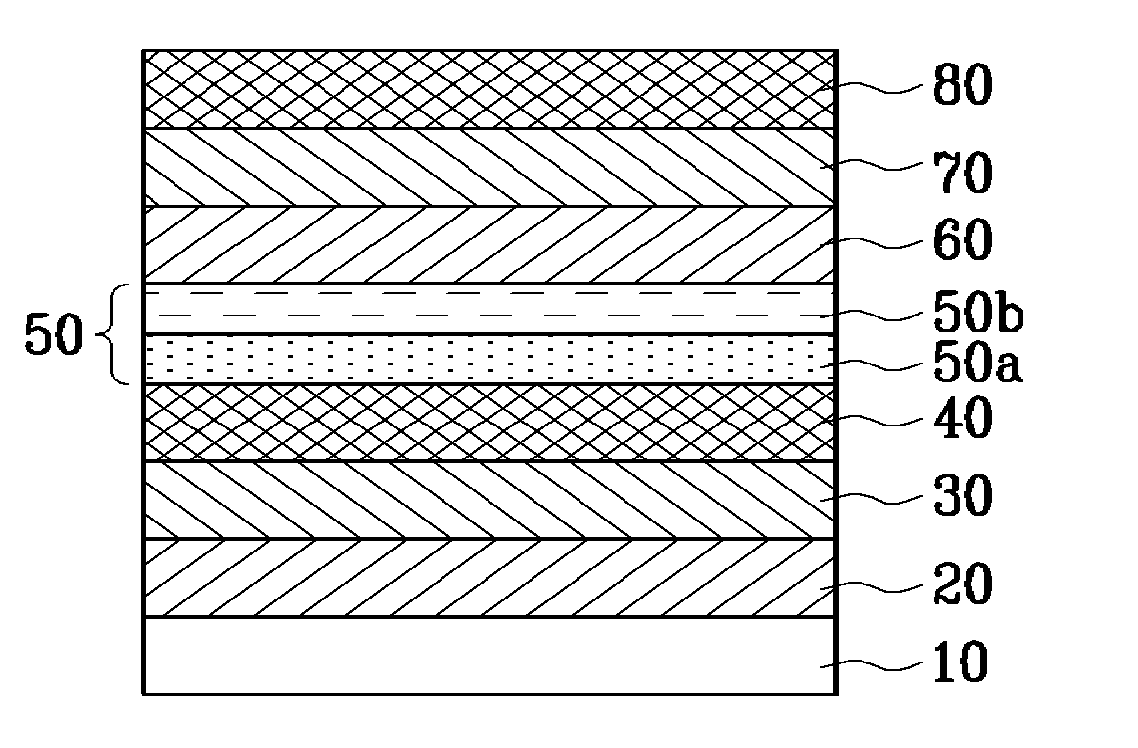
[0061] An ITO glass substrate of 15 Ω / cm2 (1,200 Å), obtained from Corning Company, is cut to a size of 50 mm×50 mm×0.7 mm. The ITO glass substrate is ultrasonically cleaned with a solution of isopropyl alcohol and pure water for 5 minutes and then cleaned with UV and ozone for 30 minutes. After the cleaning process, the ITO glass substrate is plasma-processed under vacuum of no more than 0.1 mtorr for 9 minutes.
[0062] IDE406 from Idemitsu Co. LTD is vacuum thermal deposited on the substrate to form a 700 Å thick hole injecting layer. Then, NPD is vacuum thermal deposited on the hole injecting layer to form a 150 Å thick hole transporting layer.
[0063] CBP (4,4′-biscarbazolylbiphenyl) doped with 15 wt % FIrpic is vacuum thermal deposited on the hole transporting layer to form a 300 Å thick blue emission layer. Then, a 1:1 mixture of CBP and BCP (2,9-dimethyl-4,7-diphenyl-9,10-phenanthroline) is doped with 10 wt % Ir(pq)2acac to form a 100 Å thick yellow emission layer on the blue e...
example 2
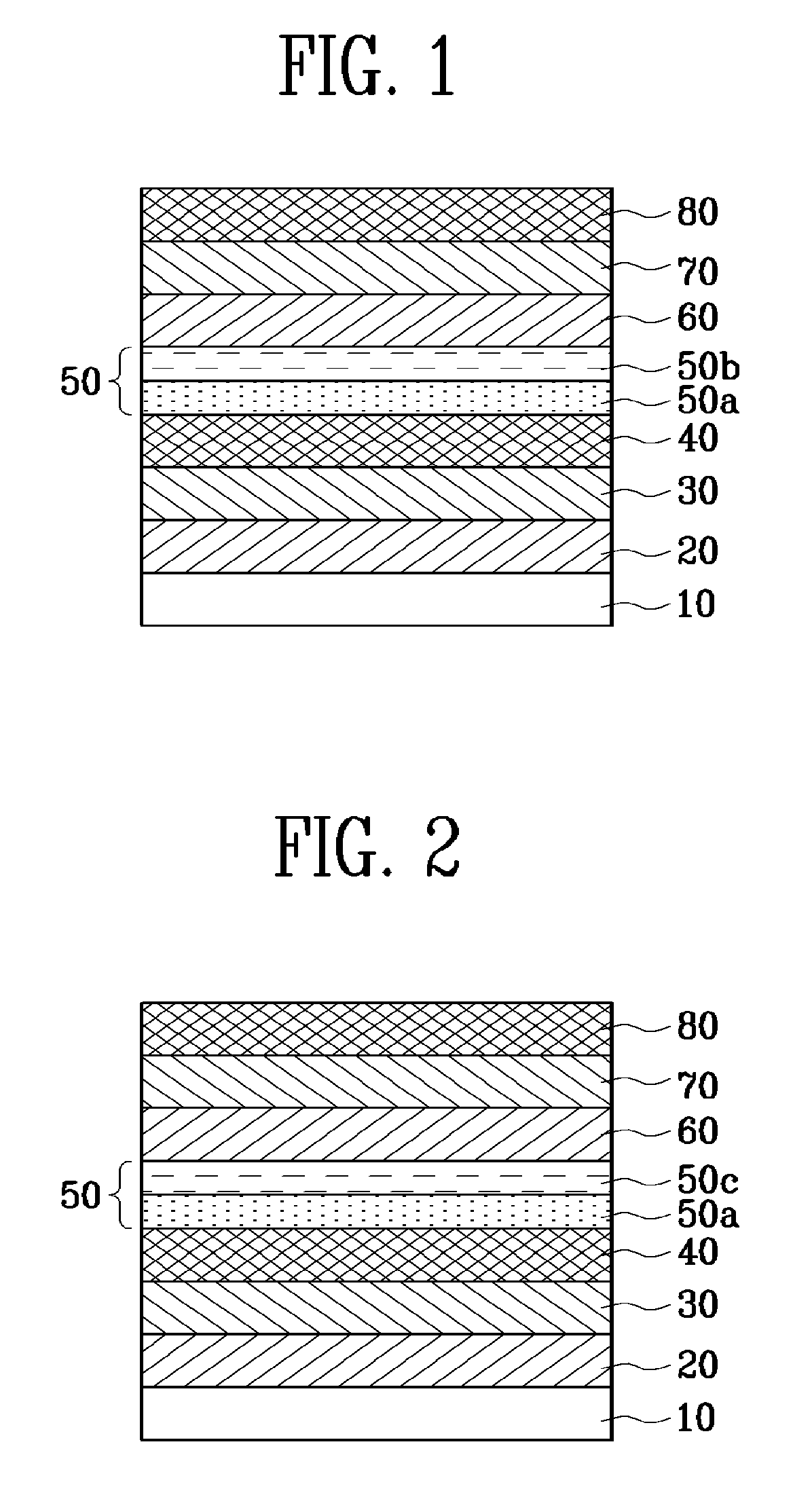
[0065] An ITO glass substrate of 15 Ω / cm2 (1,200 Ω), obtained from Corning Company, is cut to a size of 50 mm×50 mm×0.7 mm. The ITO glass substrate is ultrasonically cleaned with a solution of isopropyl alcohol and pure water for 5 minutes and then cleaned with UV and ozone for 30 minutes. After the cleaning process, the ITO glass substrate is plasma-processed under vacuum of no more than 0.1 mtorr for 9 minutes.
[0066] IDE406 from Idemitsu Co. LTD is vacuum thermal deposited on the substrate to form a 700 Å thick hole injecting layer. Then, NPD is vacuum thermal deposited on the hole injecting layer to form a 150 Å thick hole transporting layer.
[0067] CBP doped with 15 wt % FIrpic is vacuum thermal deposited on the hole transporting layer to form a 300 Å thick blue emission layer. Irppy3 and Ir(piq)2acac are mixed with each other in the ratio of 8:2. Then 10 wt % of the mixture of Trppy3 and Ir(piq)2acac is mixed with a 1:1 mixture of CBP and BCP to form a 100 Å thick green and re...
example 3
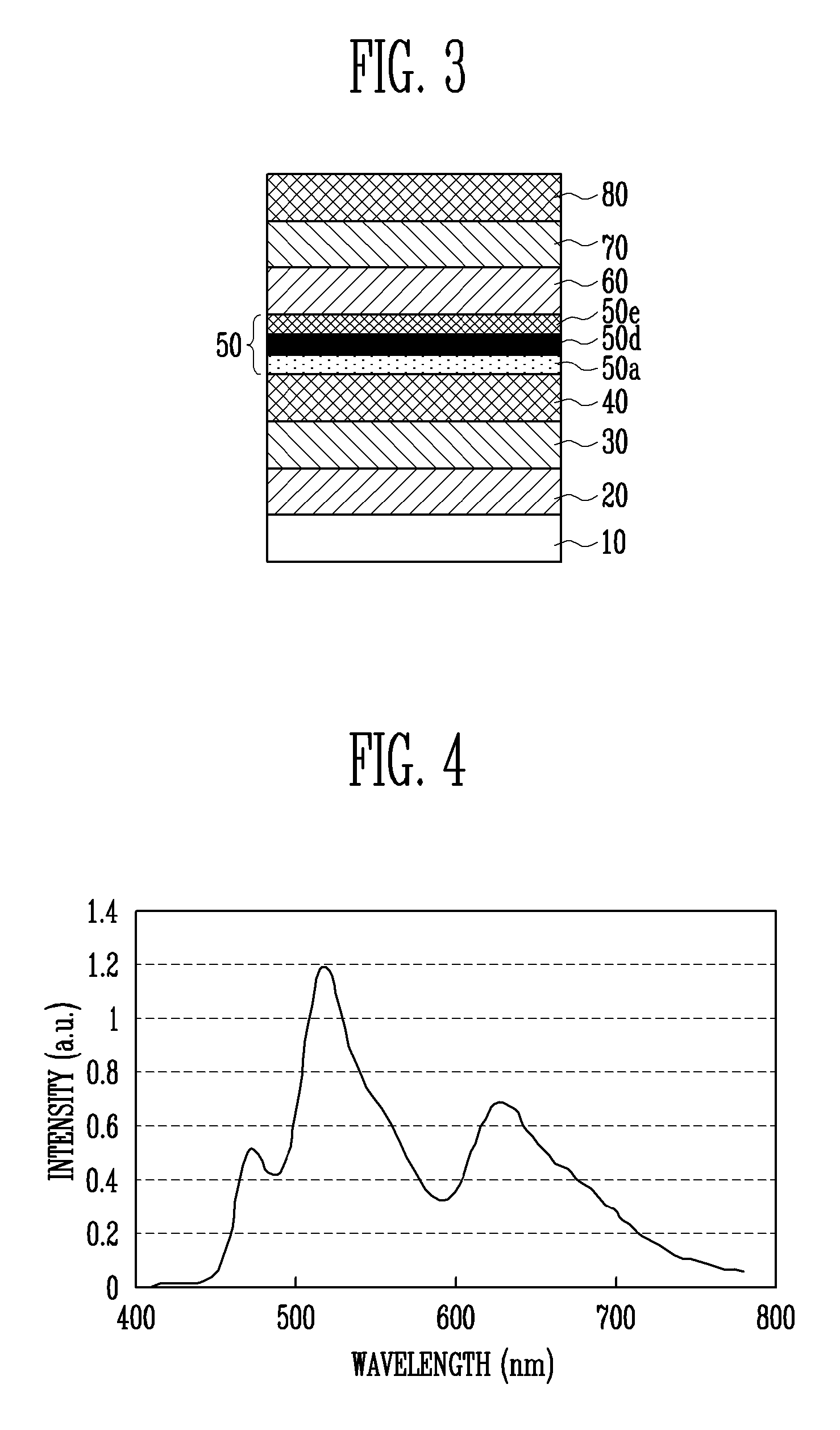
[0069] An ITO glass substrate of 15Q / cm2 (1,200A), obtained from Corning Company, is cut to a size of 50 mm×50 mm×0.7 mm. The ITO glass substrate is ultrasonically cleaned with a solution of isopropyl alcohol and pure water for 5 minutes and then cleaned with UV and ozone for 30 minutes. After the cleaning process, the ITO glass substrate is plasma-processed under vacuum of no more than 0.1 mtorr for 9 minutes.
[0070] IDE406 from Idemitsu Co. LTD is vacuum thermal deposited on the substrate to form a 700 Å thick hole injecting layer. Then, NPD is vacuum thermal deposited on the hole injecting layer to form a 150 Å thick hole transporting layer.
[0071] CBP doped with 15 wt % FIrpic is vacuum thermal deposited on the hole transporting layer to form a 300 Å thick blue emission layer. Then, a 1:1 mixture of CBP and BCP is doped with 5 wt % Irppy3 to form a 100 Å thick green emission layer on the blue emission layer by vacuum thermal deposition. Then, a 1:1 mixture of CBP and BCP is dope...
PUM
| Property | Measurement | Unit |
|---|---|---|
| Percent by mass | aaaaa | aaaaa |
| Thickness | aaaaa | aaaaa |
| Thickness | aaaaa | aaaaa |
Abstract
Description
Claims
Application Information