Liquid discharge head manufacturing method, and liquid discharge head obtained using this method
a liquid discharge head and manufacturing method technology, applied in the direction of photomechanical equipment, instruments, originals for photomechanical treatment, etc., can solve the problem of deteriorating printed images
- Summary
- Abstract
- Description
- Claims
- Application Information
AI Technical Summary
Benefits of technology
Problems solved by technology
Method used
Image
Examples
first embodiment
(First Embodiment)
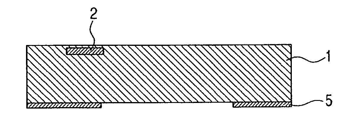
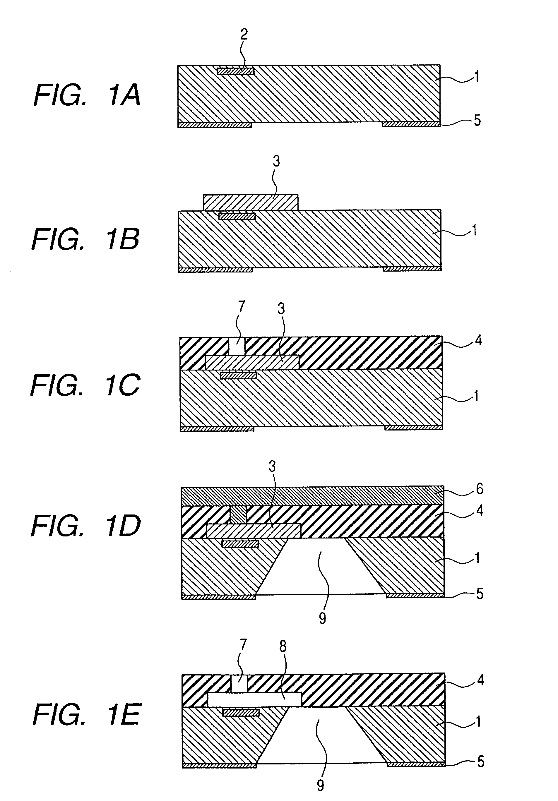
[0055]FIGS. 1A to 1E are schematic cross-sectional views showing the processing for a method according to a first embodiment of this invention for manufacturing a liquid discharge head. The method for manufacturing a liquid discharge head according to this embodiment will now be explained while referring to FIGS. 1A to 1E.
[0056] In FIG. 1A, heat generation devices 2, which are liquid discharge energy generating elements, transistors, which independently drive the heat generation devices, and a circuit (not shown), which processes data signals, for example, are mounted on a silicon substrate 1, and are electrically connected by wiring. A nitride film 5 is used as a mask for forming an ink supply port 9 that will be described later.
[0057] Then, as shown in FIG. 1B, a positive resist layer 3 is coated on the silicon substrate 1 as a dissolvable and removable solid layer, and baked. A general solvent coating method, such as spin coating or bar coating, can be employe...
second embodiment
(Second Embodiment)
[0067]FIGS. 4A to 4F are cross-sectional views for explaining example solid layer formation processing that can be employed for the present invention. A second embodiment of this invention differs from the first embodiment in that a laminated structure, for which a plurality of materials are used, is employed for the solid layer.
[0068] First, the solid layer formation processing that can be employed for this invention will be described while referring to FIGS. 4A to 4F.
[0069] As shown in FIG. 4A, a positive type resist layer 12 that contains polymethylisopropenylketone (PMIPK) as a resin element is deposited on a substrate 11. Specifically, an ODUR positive type resist is applied by spin coating, and is prebaked at 120° C. for three minutes. Then, the structure is baked at 150° C. for 30 minutes. The film thickness at this time is 15 μm. Thereafter, in order to prevent the outer edge of a wafer from being raised, Deep UV light is projected through a wafer outer ...
fourth embodiment
(Fourth Embodiment)
[0097]FIGS. 9A to 9I are diagrams showing the structure of a liquid ejection recording head according to a fourth embodiment of the present invention, and a manufacturing method therefor. In this embodiment, a liquid ejection recording head having two orifices (discharge ports) is shown; however, the same processing is applied for a high-density multi-array liquid ejection recording head having more than two orifices.
[0098] In the fourth embodiment, a substrate 201 is employed that is made, for example, of glass, ceramics, plastic or metal, as shown in FIG. 9A. FIG. 9A is a schematic perspective view of a substrate before a photosensitive material layer is formed. So long as the substrate 201 functions as a part of a wall member for a flow path, and as a support member for a flow path structure made of a photosensitive material layer that will be described later, the shape and the material of the substrate 201 are not especially limited. A desired number of liqui...
PUM
| Property | Measurement | Unit |
|---|---|---|
| thickness | aaaaa | aaaaa |
| absorbed wavelength | aaaaa | aaaaa |
| temperature | aaaaa | aaaaa |
Abstract
Description
Claims
Application Information


