Flexible printed circuit board

a printed circuit board and flexible technology, applied in the direction of printed element electric connection formation, high-frequency circuit adaptation, coupling device connection, etc., can solve the problems of difficult to improve the transmission characteristics of high-frequency signals, deterioration of high-frequency signal transmission characteristics, etc., to achieve the effect of deterioration of transmission characteristics and degrading of electrical impedance characteristics of signal lines 9

Inactive Publication Date: 2007-05-10
SONY CORP
View PDF4 Cites 47 Cited by
  • Summary
  • Abstract
  • Description
  • Claims
  • Application Information

AI Technical Summary

Benefits of technology

[0015] However, in such the flexible printed circuit board electrically connected to a connector as described in FIGS. 1-6, if the flexible printed circuit board 50 is connected to the FPC connector 7, the second wiring layer 5 having signal lines 9 exists on the side of the printed circuit board 18, as shown in FIG. 5. Accordingly, the signal lines 9 on the second wiring layer 5 and a portion, indicated by N, of the ground layer 18c on the printed circuit board 18 are coupled to each other to give rise to a degree of capacitance so that the electrical impedance characteristics of the signal lines 9 can be degraded. Thus, the electrical impedance characteristics of the signal lines 9 may fall short of a predetermined value, thereby leading to deterioration in transmission characteristics of a high-frequency signal.

Problems solved by technology

Thus, the electrical impedance characteristics of the signal lines 9 may fall short of a predetermined value, thereby leading to deterioration in transmission characteristics of a high-frequency signal.
Further, the connector for flexible printed circuit board connection disclosed in the above Japanese Patent Application Publication is of such a configuration that a flexible printed circuit board can be inserted with small degree of insertion force and, therefore, it is difficult to improve the transmission characteristics of a high-frequency signal.

Method used


Image

  • Flexible printed circuit board
  • Flexible printed circuit board
  • Flexible printed circuit board

Examples


Embodiment Construction

[0050] The following will describe preferred embodiments of a flexible printed circuit board, an optical transmitter-receiver module, and an optical transmitter-receiver in accordance with the present invention. First, a first embodiment of the flexible printed circuit board of the present invention will be described.

[0051] (Configuration of the flexible printed circuit board according to the first embodiment of the present embodiment)

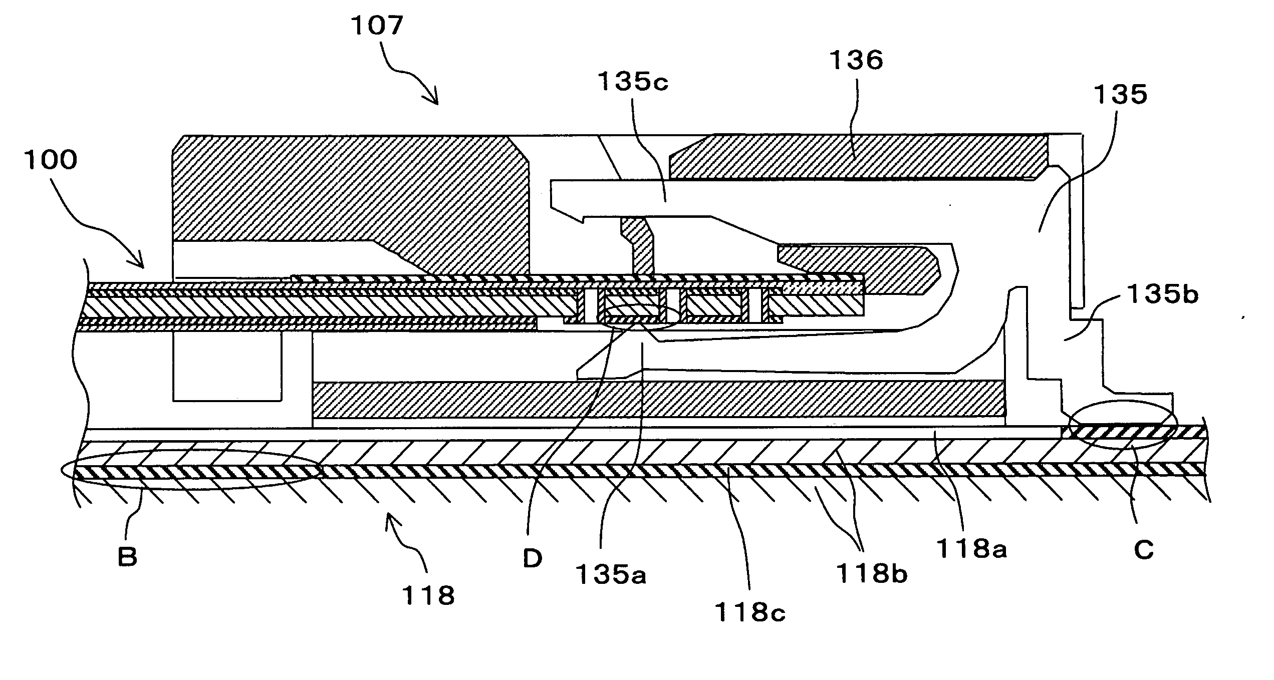
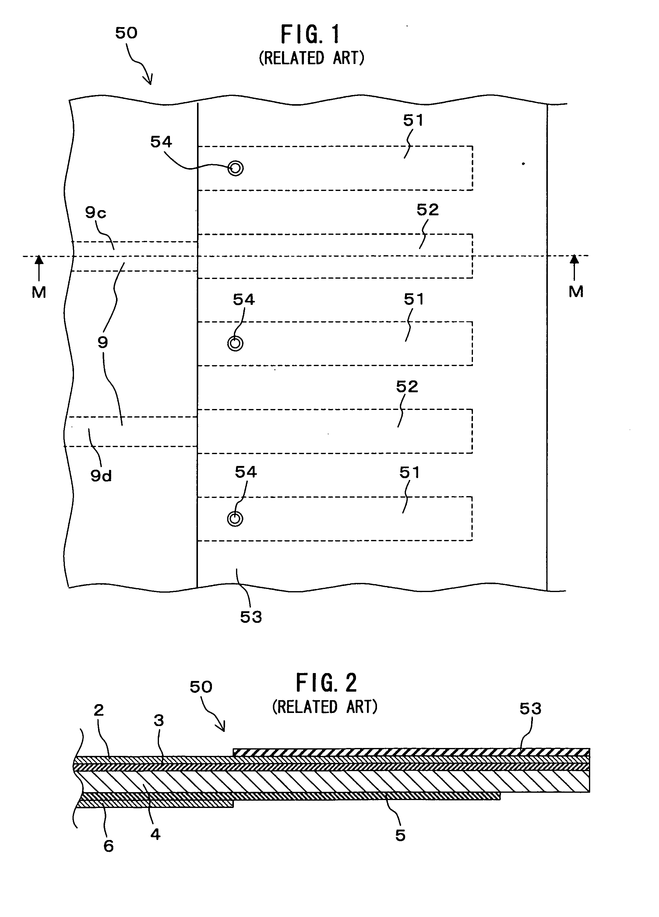
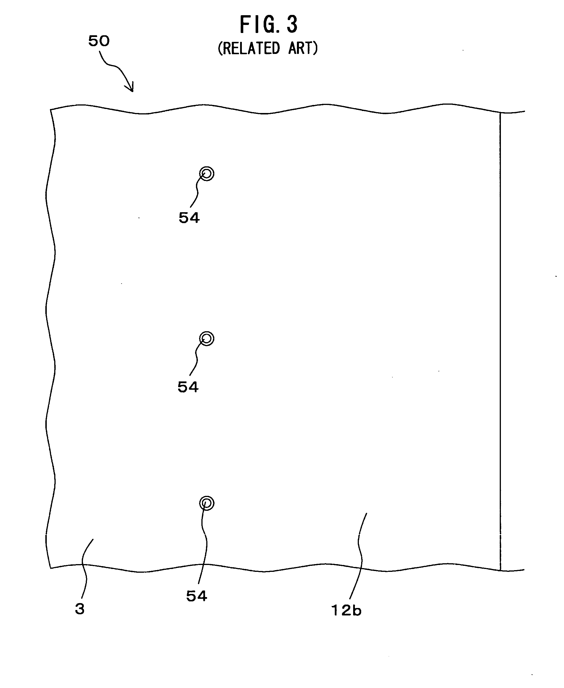
[0052]FIGS. 7-11 are explanatory views of a configuration of a flexible printed circuit board 100 according to a first embodiment of the present invention. FIG. 7 is a plan view of the flexible printed circuit board 100 for showing an outline thereof, a part of which configuration is indicated, in a transparent condition, by a broken line for purposes of clarification. FIG. 8 is a cross-sectional view of the flexible printed circuit board 100 according to the first embodiment of the present invention taken along lines A-A of FIG. 7. FIG. 9 is a plan ...


PUM

PropertyMeasurementUnit
diametersaaaaaaaaaa
widthaaaaaaaaaa
widthaaaaaaaaaa

Abstract

A flexible printed circuit board has an insulation layer, a first signal wiring layer including a microstrip line, a second signal wiring layer including a signal connection terminal for allowing the microstrip line to connect the exterior connector electrically, and a ground conductive section having a ground connection terminal for connecting the exterior connector. The microstrip line and the signal connection terminal are connected to each other by a wiring via hole. The wiring via hole passes through the insulation layer, the first signal wiring layer, and the second signal wiring layer. The microstrip line has a taper section which gradually enlarges a width of the microstrip line toward the wiring via hole in the vicinity of the wiring via hole. The ground conductive section that corresponds to the microstrip line has a taper section with a shape matching the taper section of the microstrip line.

Description

CROSSREFERENCE TO RELATED APPLICATION [0001] The present invention contains subject matter related to Japanese Patent Application JP 2005-317101 filed in the Japanese Patent Office on Oct. 31, 2005, the entire contents of which being incorporated herein by reference. BACKGROUND OF THE INVENTION [0002] 1. Field of the Invention [0003] The present invention relates to a flexible printed circuit board, and to an optical transmitter-receiver module and an optical transmitter-receiver which are each equipped with such a flexible printed circuit board. [0004] 2. Description of Related Art [0005] For electrically connecting a flexible printed circuit board with other types of board or the like, a method has been used to connect them by means of a connector for connecting the flexible printed circuit board. Further, for transmitting high-frequency signals over a printed circuit board, a printed circuit board with a microstrip line structure has been employed. [0006]FIGS. 1-4 are explanatory...

Claims


Application Information

Patent Timeline
Patent Type & Authority Applications(United States)
IPC IPC(8): H01L23/52H01R12/79H04B10/40H04B10/50H04B10/60H04B10/66
CPCH05K1/0219H05K1/0237H05K1/118H05K3/42H05K2201/093H05K2201/09481Y10T29/4913H05K2201/09727H01R12/79H05K2201/09381H05K2201/09409Y10T29/49155H05K2201/09618H01R12/77H04B10/40
Inventor MUTO, AKIRATANAKA, TOMOKAZU
Owner SONY CORP
Why Eureka
Try Eureka