[0012] However, where the above-described protective film is formed by a CVD process as described previously, it may be necessary to remove the portions of the protective film overlying the external connector terminals after forming the protective film over the whole area of the substrate. This complicates the fabrication sequence. Furthermore, when the protective film is etched by an RIE process, in a case where NF3 gas is used as the etchant gas as described previously, there is the problem that the fabrication cost is high because the NF3 gas is expensive. In addition, the protective film made of SiNx may be removed by wet
etching using a strong acid but there is the possibility that even the protective film overlying the display area is overetched. Further, where a film of SiNx is formed by a CVD process, poisonous monosilane is used as process gas and, therefore, the
process equipment may require a device for detoxifying the process gas to prevent effects on the
human body. In addition, a pumping
system may also be necessary to adjust the pressure of the process environment. Consequently, the structure of the equipment is complex. This also increases the fabrication cost.
[0013] The film quality of the protective film made of SiNx is different according to different
reaction conditions. For example, in a display device having a protective film (
environmentally friendly SiNx film) to enhance the
film density for preventing formation of dark spots due to ingress of
moisture into the OEDs, for example, under high-temperature, high-
humidity environments, generation and growth of the dark spots are suppressed when stored under high-temperature, high-humidity environments. However, increasing the
film density increases the stress in the protective film, producing peeling of the film. This shortens the emission lifetime. On the other hand, where a protective film having
low stress (life-prioritized SiNx film) is formed to prolong the emission lifetime, the emission life can be increased successfully but the film density of the protective film drops. Consequently, where the device is stored under high-temperature, high-humidity environments, dark spots are enlarged. Additionally, a technique for forming a protective film from lamination
layers of the aforementioned
environmentally friendly SiNx film and life-prioritized SiNx film according to the purpose has been discussed. However, the tact time is long. The
process equipment is complicated and the cost is increased.
[0015] Accordingly, it is desirable to provide a method of fabricating a display device which can be fabricated using a simplified fabrication sequence at a reduced cost, has a long emission lifetime, and exhibits long durability even under high-temperature, high-humidity environments. It is also desirable to provide this display device.
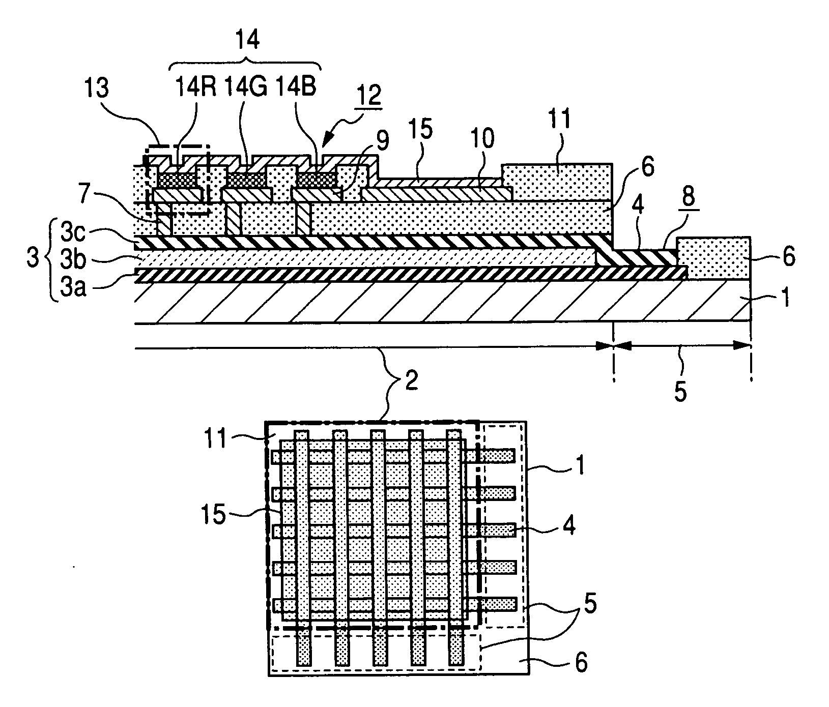
[0018] According to this method of fabricating the display device, the protective film is selectively formed on the display region of the substrate by a method of application. Consequently, the surfaces of the external connector terminals are maintained exposed. This would make it unnecessary to etch away the portions of the protective film overlying the external connector terminals after formation of the protective film. Hence, the fabrication sequence is simplified. Furthermore, since the protective film is formed by the method of application, it may be unnecessary to use a poisonous process gas, unlike the case where a protective film of SiNx is formed by a CVD process as described previously. Also, it may be unnecessary to adjust the pressure of the process environment. This may make it unnecessary to install a device for detoxifying the process gas or pumping
machine within the process equipment. In consequence, the structure of the equipment is simplified.
[0019] It has been confirmed that the display device having the protective film formed by a method of application in accordance with the aforementioned method of fabrication has longer emission lifetime and longer durability even under high-temperature, high-humidity environments than a display device having a protective film of SiNx fabricated by a CVD method as already described previously. This will be set forth in detail in the description of embodiments of the invention.
[0020] As described so far, according to the method of fabricating a display device according to an embodiment of the invention and the resulting display device, the fabrication sequence is simplified. The
machine for fabricating the protective film is simplified. This shortens the tact time. In addition, the fabrication cost can be suppressed. Accordingly, the productivity can be improved. Furthermore, the display device has a long emission lifetime and shows long durability even under high-temperature, high-humidity environments and so images of high quality can be displayed.

