Method and system for adaptively controlling a laser-based material processing process and method and system for qualifying same

a laser-based material and processing process technology, applied in the laser field, can solve problems such as limit yield, and achieve the effect of eliminating unnecessary test steps in device fabrication

Inactive Publication Date: 2007-05-10
ELECTRO SCI IND INC
View PDF51 Cites 71 Cited by
  • Summary
  • Abstract
  • Description
  • Claims
  • Application Information

AI Technical Summary

Benefits of technology

[0015] There is a need for an improved laser-based repair system to increase yield of various semiconductor manufacturing processes.
[0016] It is desirable to eliminate unnecessary test steps in device fabrication.

Problems solved by technology

However, intermittent checks limit yield.

Method used


Image

  • Method and system for adaptively controlling a laser-based material processing process and method and system for qualifying same
  • Method and system for adaptively controlling a laser-based material processing process and method and system for qualifying same
  • Method and system for adaptively controlling a laser-based material processing process and method and system for qualifying same

Examples


Embodiment Construction

)

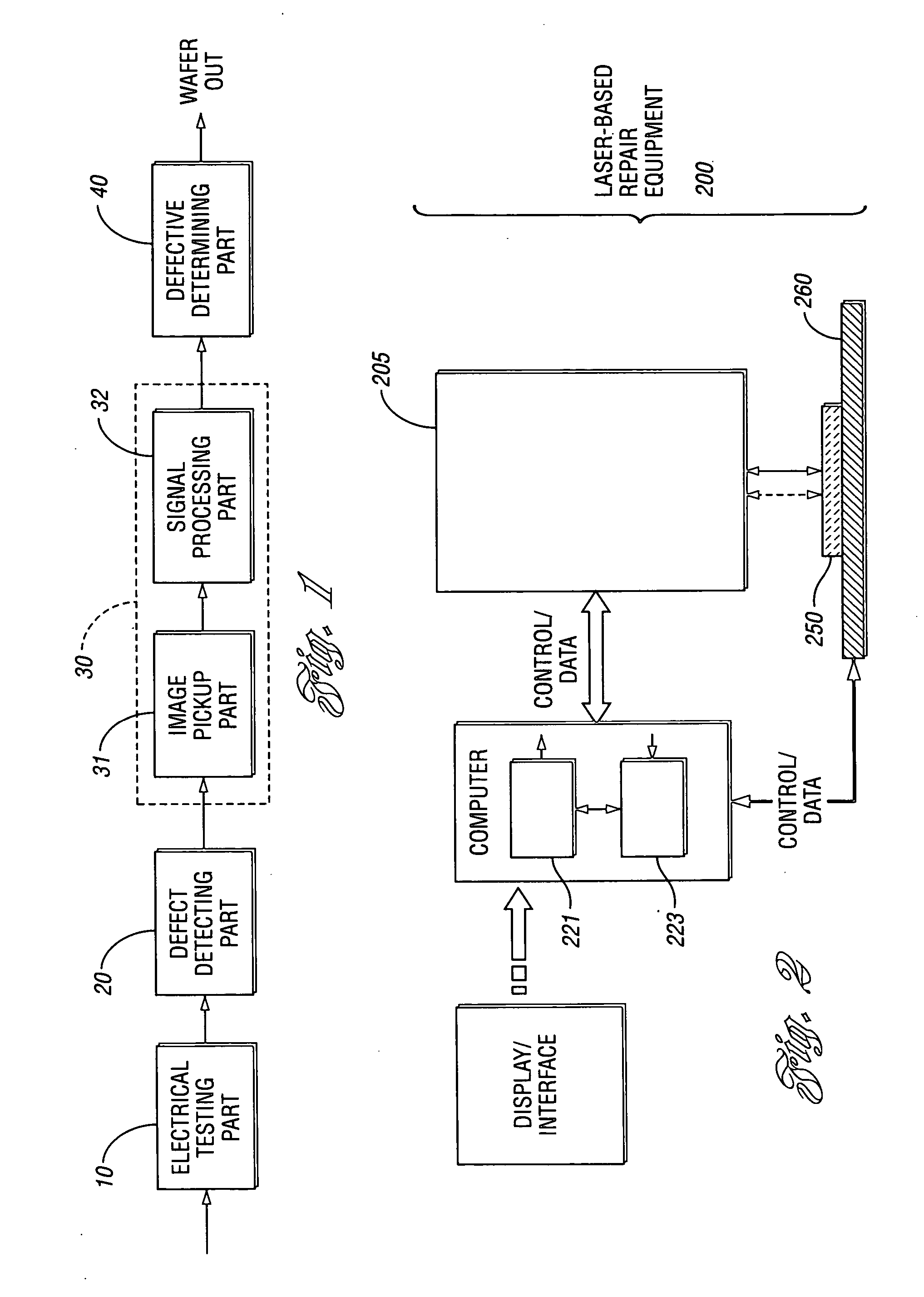
[0085] Unless otherwise stated the phrase “semiconductive workpiece” or terms “workpiece” or “substrate” are to be non-limiting, and are to be construed as a workpiece having a semiconductor material. By way of example, a workpiece may be a semiconductor wafer with a plurality of die thereon, and may generally include multi-material devices. Memory circuits fabricated on silicon substrates are one example, and are generally constructed as a series of layers on a silicon wafer as taught in LIA HANDBOOK (referenced above), U.S. Pat. Nos. 5,936,296; 6,320,243; and 6,518,140, and numerous other patents and publications. The workpiece may be an entire substrate (e.g., 200 mm diameter wafer) with a large number of die, singulated die or devices, device portions, or other variations of semiconductor devices or chips which may repaired with a laser.

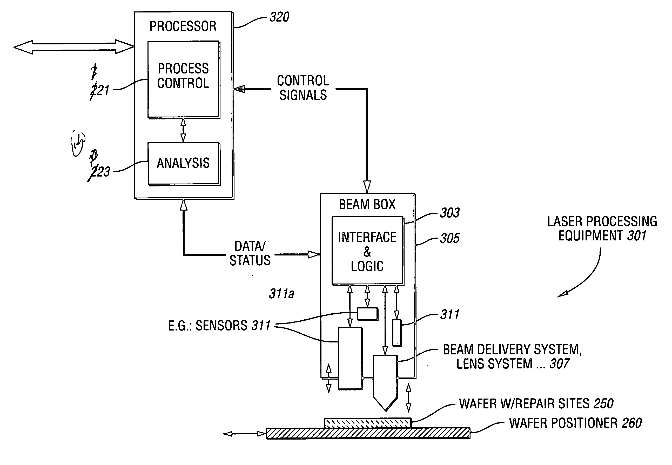
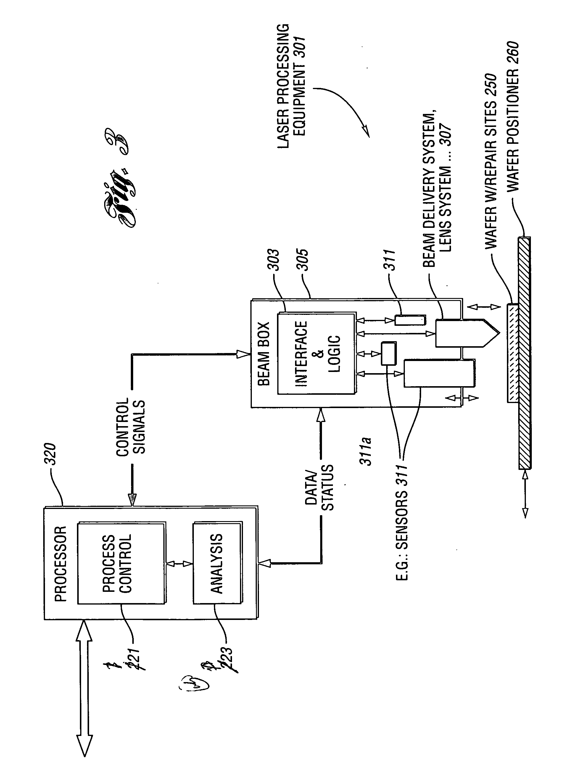
[0086]FIG. 2 shows some elements of a general embodiment of the present invention. The laser-based repair system 200 generally includes laser ...


PUM

PropertyMeasurementUnit
diameteraaaaaaaaaa
widthaaaaaaaaaa
sizeaaaaaaaaaa

Abstract

A method and system for adaptively controlling a laser-based material processing process are provided. The system includes sensing equipment to measure a process variable or condition of at least one of a laser-based material processing system and a workpiece processed by the material processing system and to provide a corresponding measurement signal. The control system also includes a signal processor for processing the measurement signal to obtain a processed signal which initiates, at least semi-automatically, an action associated with at least one of the material processing system and the workpiece. A method and system for at least semi-automatically qualifying a laser-based material processing system which delivers laser energy to locations on or adjacent a plurality of microstructures formed on a workpiece to at least partially process the microstructures are also provided.

Description

CROSS-REFERENCE TO RELATED PATENTS AND PUBLISHED PATENT APPLICATIONS [0001] This application claims the benefit of U.S. provisional patent application Ser. No. 60 / 810,964 filed Jun. 5, 2006. [0002] Except where indicated, the following patents and patent applications are assigned to the assignee of the present invention and are hereby incorporated by reference in their entirety herein: U.S. Pat. No. 6,972,268 (the '268 patent); U.S. Pat. No. 6,949,844 (the '844 patent); U.S. Pat. No. 6,911,622 (the '622 patent); U.S. Pat. No. 6,878,899 (the '899 patent); U.S. Pat. No. 6,727,458 (the '458 patent); U.S. Pat. No. 6,573,473 (the '473 patent); published PCT Application No. WO 2004 / 114192 (the '4192 publication); published U.S. Patent Publication No. 2005 / 0150880 (the '0880 publication); and U.S. Pat. No. 6,987,786 (the '786 patent).BACKGROUND OF THE INVENTION [0003] 1. Field of the Invention [0004] The present invention relates to a method and system for adaptively controlling a laser-ba...

Claims


Application Information

Patent Timeline
Patent Type & Authority Applications(United States)
IPC IPC(8): G06F19/00B23K26/38B23K26/03
CPCB23K26/032H01L22/24H01L23/5258G05B11/01G05B15/02H01L2924/0002H01L2924/00B23K26/36H01S5/06
Inventor GRIFFITHS, JOSEPH J.PELSUE, KURT
Owner ELECTRO SCI IND INC
Why Eureka
Try Eureka