Test Pads, Methods and Systems for Measuring Properties of a Wafer

a technology of test pads and insulating films, applied in the direction of individual semiconductor device testing, semiconductor/solid-state device testing/measurement, instruments, etc., can solve the problems of increasing the probability that the process will be within the process limits, the need for direct physical electrical contact with the insulating film is particularly undesirable, and the method that utilizes monitor wafers is becoming increasingly undesirabl

Inactive Publication Date: 2007-05-17
KLA TENCOR TECH CORP
View PDF87 Cites 46 Cited by
  • Summary
  • Abstract
  • Description
  • Claims
  • Application Information

AI Technical Summary

Benefits of technology

[0015] One embodiment relates to a test pad formed on a wafer. The test pad includes a test structure configured such that one or more electrical properties of the test structure can be measured. The test pad also includes a conductive layer formed between the test structure and the wafer. The conductive layer prevents structures located under the test structure between the conductive layer and the wafer from affecting the one or more electrical properties of the test structure during measurement.
[0024] An additional embodiment relates to a different test pad formed on a wafer. This test pad includes a gate structure configured such that one or more electrical properties of the gate structure can be measured. The test pad also includes an isolated insulator pad formed between the gate structure and the wafer. The isolated insulator pad prevents structures located under the gate structure between the isolated insulator pad and the wafer from affecting the one or more electrical properties of the gate structure during measurement.

Problems solved by technology

However, the necessity of direct physical electrical contact with the insulating film is particularly undesirable in many manufacturing situations.
Therefore, such a method may increase the probability that the process will be within process limits when product wafers are processed.
As the value of semiconductor wafers increases, and the demand for better throughput and more efficient tool usage increases, methods that utilize monitor wafers are becoming increasing undesirable.
For example, methods that include processing and measuring a monitor wafer require materials and labor to create and measure the monitor wafer thereby increasing manufacturing costs and reducing throughput.
In addition, measurements performed on monitor wafers may not accurately reflect properties of product wafers for a number of reasons.
Therefore, a process may not be accurately evaluated, monitored, and controlled using measurements performed on a monitor wafer.
These corona applications are typically relatively large scale in nature, and the industrial applications for which they are designed are also relatively insensitive to the level of corona, the species being produced, and the production of byproduct species.
This particular application of corona technology is sensitive to variations in corona deposition and contamination from corona deposition.
Corona generation in ambient conditions, however, may produce a number of undesirable byproducts.
In addition, the electric fields and high voltages may attract particulates into the vicinity of the corona source.
In a conventional corona deposition system, such byproducts and particulates may accumulate over time and may deposit onto a wafer and / or change the production of species being created.
Therefore, such byproducts and particulates may reduce the accuracy of measurements performed on a semiconductor wafer using a corona source, the accuracy of alterations made to a process using such measurements, and the yield of semiconductor manufacturing processes monitored and altered using a corona source for measurements of electrical properties.

Method used


Image

  • Test Pads, Methods and Systems for Measuring Properties of a Wafer
  • Test Pads, Methods and Systems for Measuring Properties of a Wafer
  • Test Pads, Methods and Systems for Measuring Properties of a Wafer

Examples


Embodiment Construction

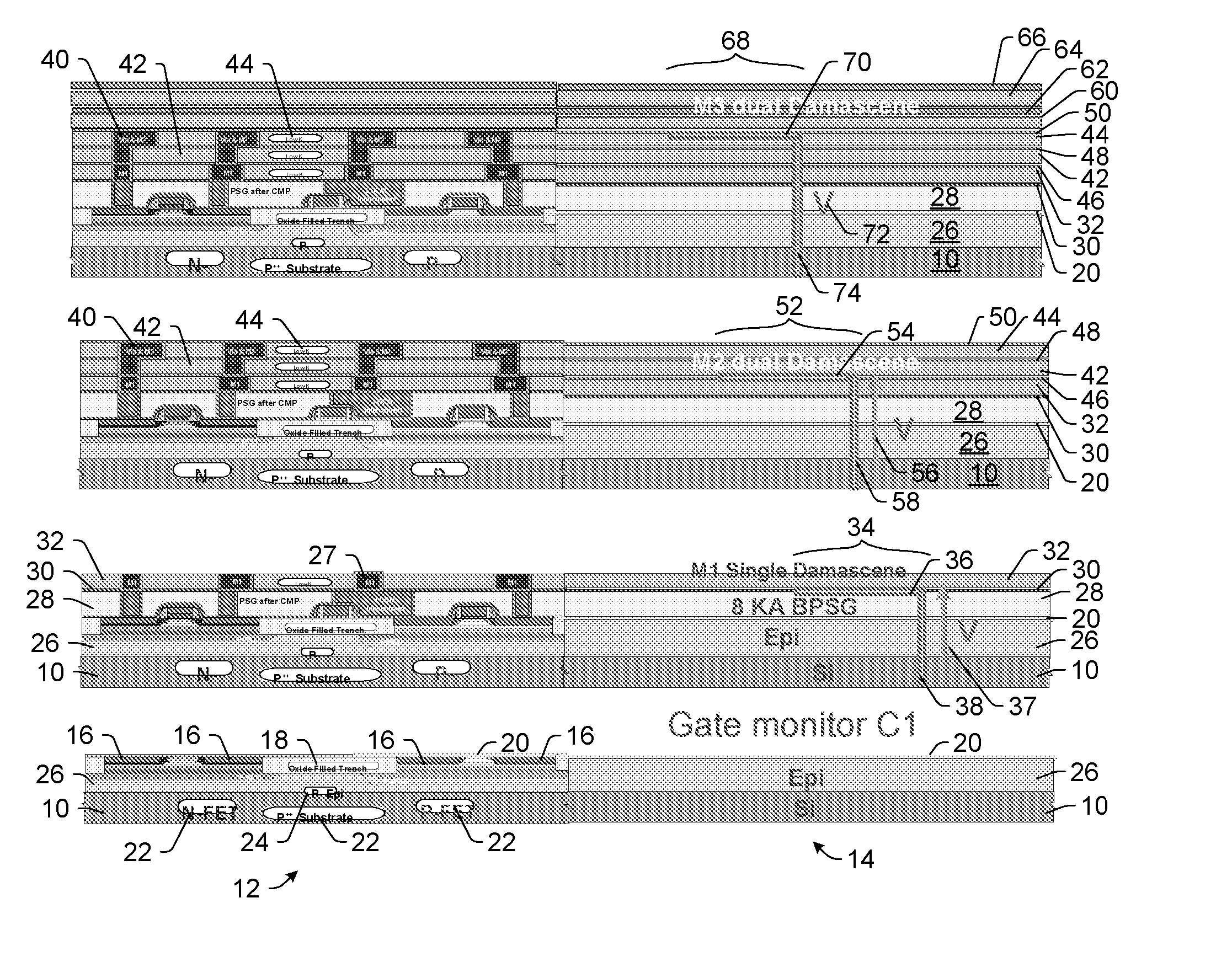
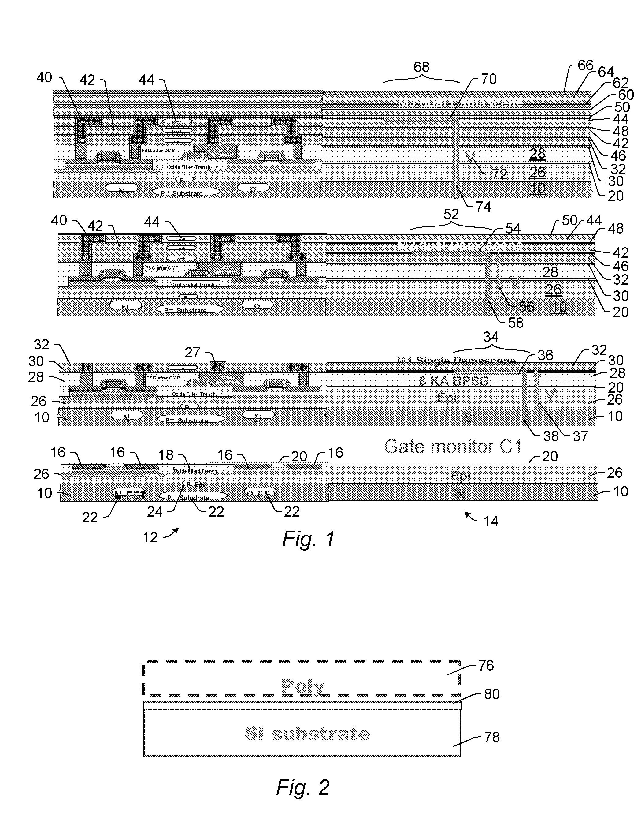
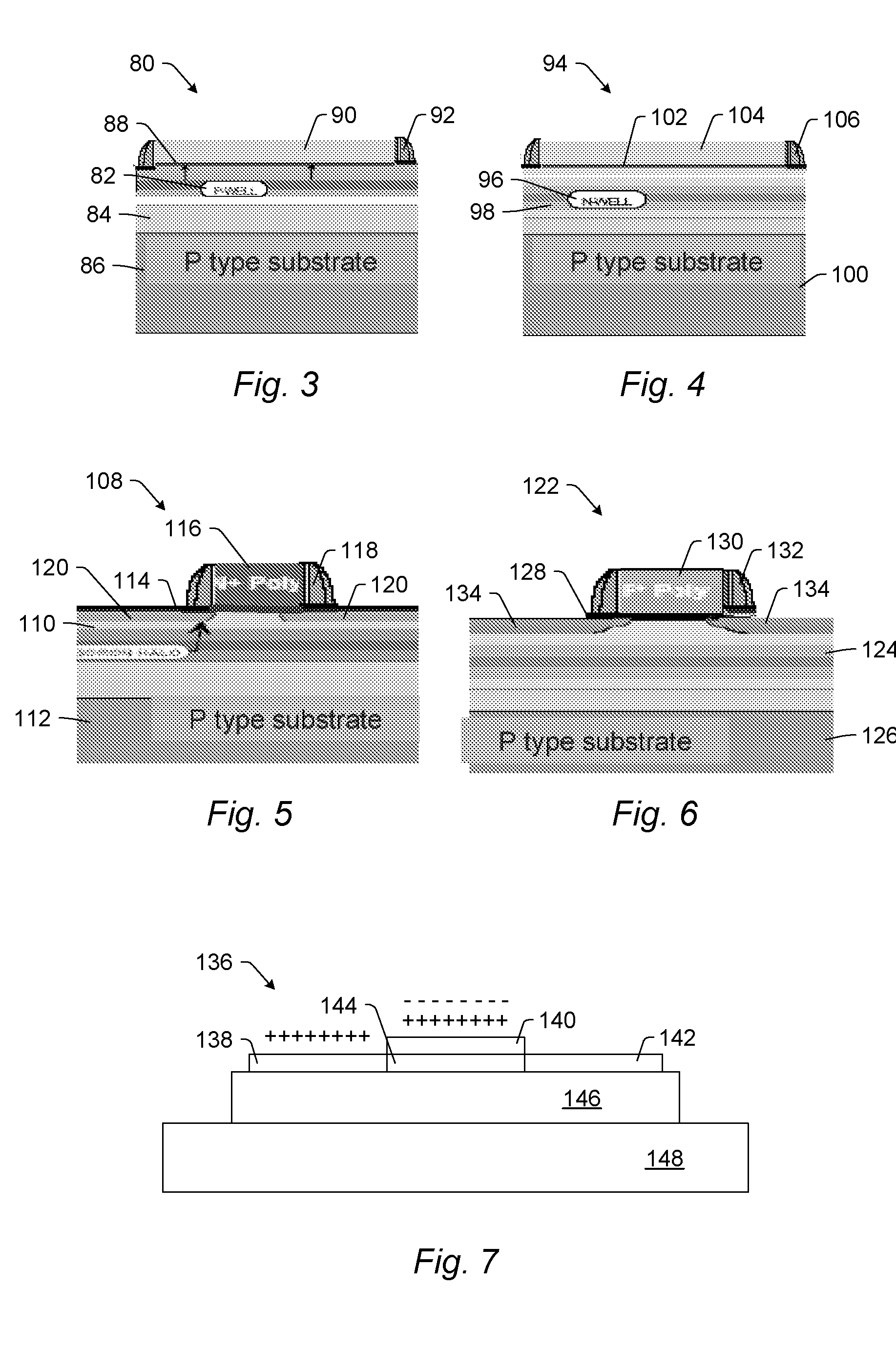
[0136] As used herein, the term “wafer” generally refers to substrates formed of a semiconductor or non-semiconductor material. Examples of such a semiconductor or non-semiconductor material include, but are not limited to, monocrystalline silicon, gallium arsenide, and indium phosphide. Such substrates may be commonly found and / or processed in semiconductor fabrication facilities.

[0137] One or more layers may be formed upon a wafer. For example, such layers may include, but are not limited to, a resist, a dielectric material, and a conductive material. Many different types of such layers are known in the art, and the term wafer as used herein is intended to encompass a wafer on which all types of such layers may be formed. One or more layers formed on a wafer may be patterned. For example, a wafer may include a plurality of dies, each having repeatable patterned features. Formation and processing of such layers of material may ultimately result in completed semiconductor devices. ...


PUM


Abstract

Test pads, methods, and systems for measuring properties of a wafer are provided. One test pad formed on a wafer includes a test structure configured such that one or more electrical properties of the test structure can be measured. The test pad also includes a conductive layer formed between the test structure and the wafer. The conductive layer prevents structures located under the test structure between the conductive layer and the wafer from affecting the one or more electrical properties of the test structure during measurement. One method for assessing plasma damage of a wafer includes measuring one or more electrical properties of a test structure formed on the wafer and determining an index characterizing the plasma damage of the test structure using the one or more electrical properties.

Description

PRIORITY CLAIM [0001] This application claims priority to U.S. Provisional Application No. 60 / 709,736 entitled “Test Pads, Methods, and Systems for Measuring Properties of a Wafer, and Systems and Methods for Controlling Deposition of a Charge on a Wafer for Measurement of One or More Electrical Properties of the Wafer,” filed Aug. 19, 2005, which is incorporated by reference as if fully set forth herein.BACKGROUND OF THE INVENTION [0002] 1. Field of the Invention [0003] The present invention generally relates to test pads, methods, and systems for measuring properties of a wafer. Certain embodiments relate to methods for assessing plasma damage of a wafer. Other embodiments relate to methods and systems for controlling deposition of a charge on a wafer for measurement of one or more electrical properties of the wafer. [0004] 2. Description of the Related Art [0005] The following description and examples are not admitted to be prior art by virtue of their inclusion in this section. ...

Claims


Application Information

Patent Timeline
Patent Type & Authority Applications(United States)
IPC IPC(8): G01R31/02
CPCG01R31/2831G01R31/2856H01L22/34H01L2924/0002H01L2924/00
Inventor SHI, JIANOUZHANG, XIAFANGPEI, SHIYOUHUANG, SHU CHUNYEH, DENNISRZEPIELA, JEFFREY A.FENG, YIPINGKHAN, AHMAD
Owner KLA TENCOR TECH CORP
Why Eureka
Try Eureka