Solid-state imaging device for high-speed photography

Active Publication Date: 2007-05-17
PANASONIC CORP
View PDF7 Cites 38 Cited by
  • Summary
  • Abstract
  • Description
  • Claims
  • Application Information

AI Technical Summary

Benefits of technology

[0011] Therefore, with the foregoing problems of the related art in mind, it is an object of the present invention to provide a solid-state imaging device for high-speed photo

Problems solved by technology

That is, there is a limit to the number of shots that a digital high-speed camera can photograph continuously because of restrictions of a writing speed to a recording medium or the like.
On the other hand, when the photography is to be conducted with a high resolution and with a high speed, the number of frames that the camera can photograph is limited and the photographing time will be extremely short because the photography sho

Method used


Image

  • Solid-state imaging device for high-speed photography
  • Solid-state imaging device for high-speed photography
  • Solid-state imaging device for high-speed photography

Examples


Example

EMBODIMENT 1

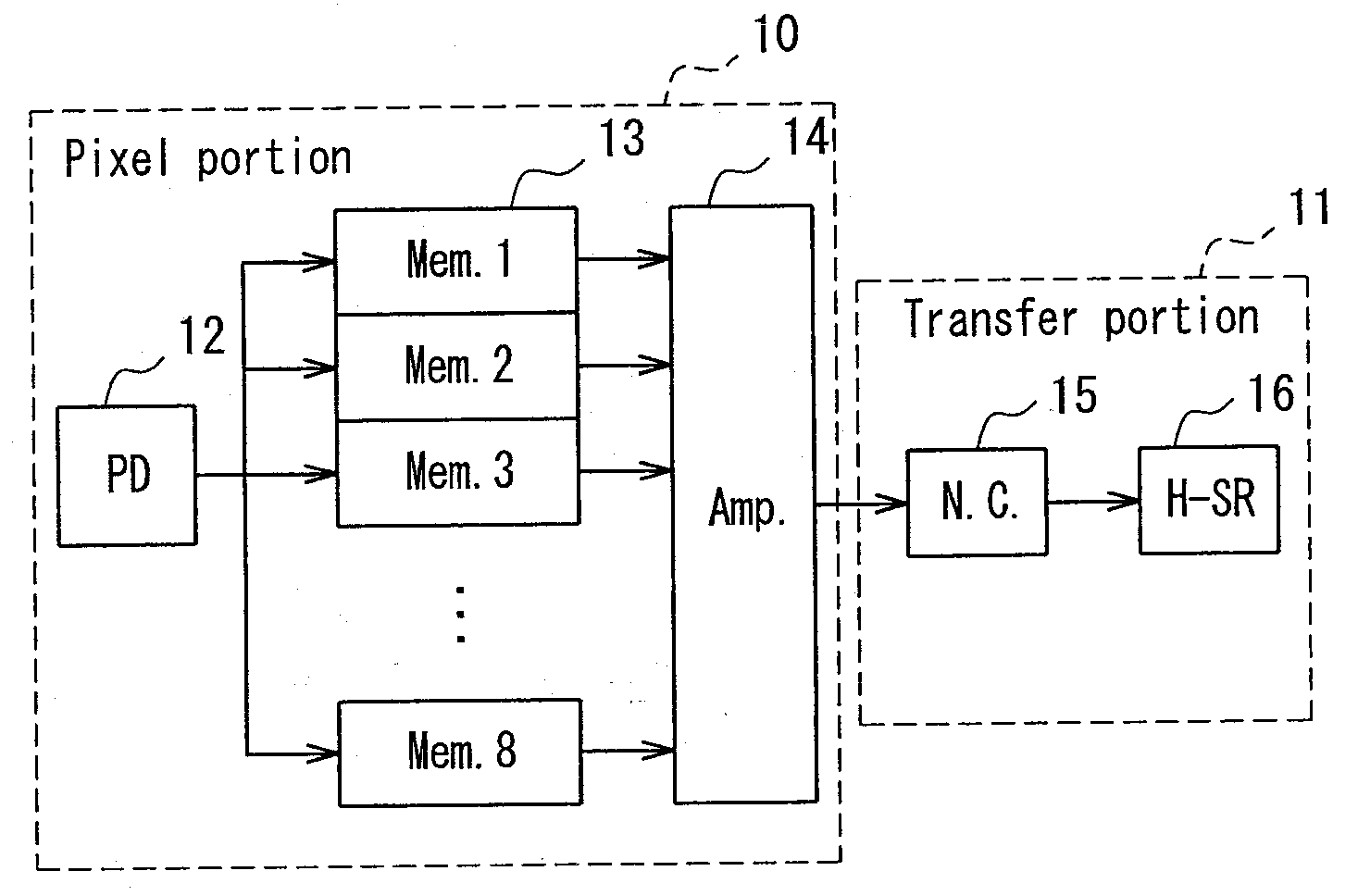
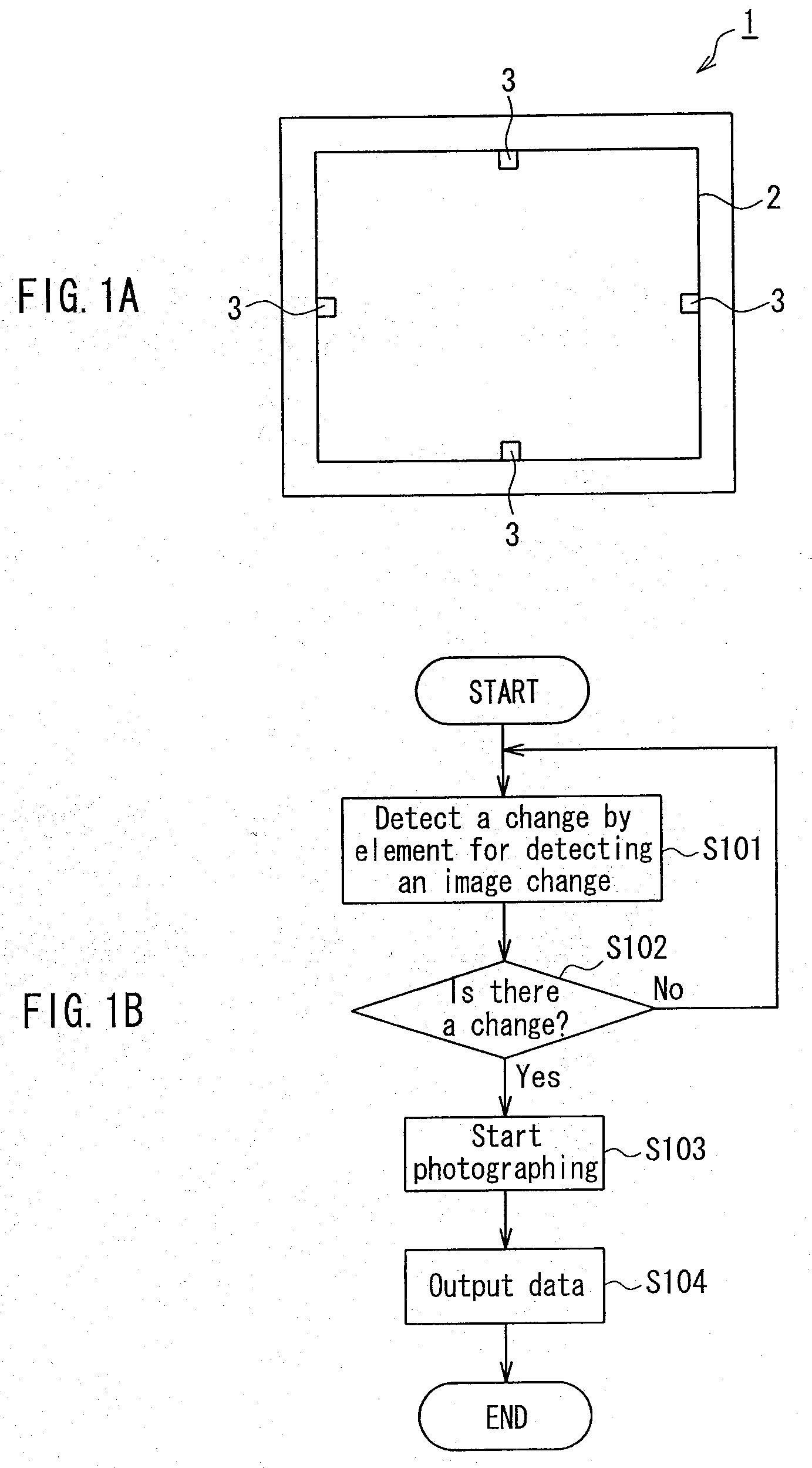
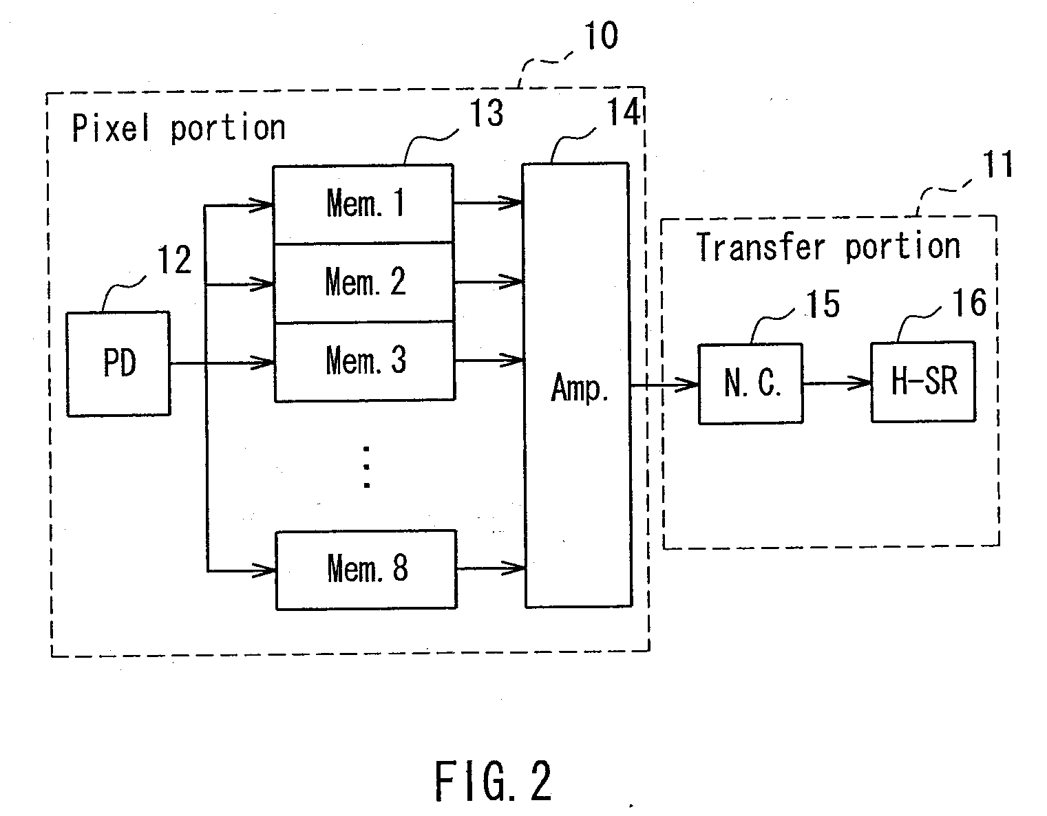
[0047]FIG. 1A is a plan view schematically showing the configuration of a solid-state imaging device 1 for a high-speed camera according to Embodiment 1 of the present invention. The solid-state imaging device 1 includes a plurality of photodetectors for photography disposed in a matrix form to correspond to pixels in a rectangular imaging element area 2. At predetermined positions of the imaging element area 2, four change detection elements 3 are disposed for detecting a change in a target of the photography (image). Herein, the change detection elements 3 may be disposed at predetermined positions of an area surrounding the imaging element area 2. For example, the change detection elements 3 may be formed on the same semiconductor substrate as of the imaging element area 2 and be disposed so as to surround the periphery of the imaging element area 2. Alternatively, the change detection elements 3 may be disposed periodically in the imaging element area with constant ...

Example

EMBODIMENT 2

[0073] Referring now to FIGS. 9 to 11, a solid-state imaging device for high-speed camera according to Embodiment 2 of the present invention will be described below. The basic configuration of the solid-state imaging device of the present embodiment is similar to that of Embodiment 1, but the present embodiment has an improved configuration, i.e., information from change detection elements is analyzed, and when detection signals in a specific combination are obtained, the starting or stopping of the photographing is controlled. The explanation of such improvement follows.

[0074] When the change detection elements are provided to detect a change in image and the photographing simply is started or stopped automatically in accordance with the detection signal as a trigger as in Embodiment 1, there is a possibility that a malfunction occurs due to camera shake, a change in ambient lighting of a photographing target or the like. Since the change detection elements detect eve...

Example

EMBODIMENT 3

[0081] Referring now to FIGS. 12 and 13, a solid-state imaging device for high-speed camera according to Embodiment 3 of the present invention will be described below. In the present embodiment, an imaging element area (solid-state imaging element) and a change detection element are provided separately. An optical system is provided for splitting light incident on the imaging element area and letting a part of the split light be incident on the change detection element.

[0082]FIG. 12 shows the state where light incident on a solid-state imaging element 29 is split by a prism 30. Light passing through a lens 31 is split into light that travels in a straight line through the prism 30 and is incident on the solid-state imaging element 29 having an imaging element area and light that is bent by the prism 30 and is incident on a change detection element 3.

[0083] In this way, the light incident on pixels is split into the light incident on the solid-state imaging element 29 ...


PUM


Abstract

A solid-state imaging device for high-speed photography includes an imaging element area in which a plurality of pixel portions having photodetectors for photography are disposed in a matrix form. The solid-state imaging device generates image data by capturing pixel information obtained from the photodetectors for photography. The solid-state imaging device for high-speed photography further includes: a change detection element that detects a change in an amount of incident light, which is disposed in the imaging element area or at a predetermined position surrounding the imaging element area; and a controller that controls starting or stopping of capturing of pixel information obtained from the photodetectors for photography in accordance with a trigger signal based on a detection signal output from the change detection element. Since the photographing can be started in accordance with the generation of a phenomenon, the phenomenon can be recorded with reliability, and an excellent power-saving capability also can be provided.

Description

BACKGROUND OF THE INVENTION [0001] 1. Field of the Invention [0002] The present invention relates to a solid-state imaging device with a plurality of photodetectors disposed in a matrix form to correspond to pixels. More particularly, the present invention relates to a solid-state imaging device provided with a function suited for the use as a high-speed camera. [0003] 2. Description of Related Art [0004] A high-speed camera is used for detailed analysis of the test results for crash tests of vehicles, drop tests of products and the like. In recent years, a high-speed camera especially is used also for analysis of a phenomenon in the physical chemistry field including for the analysis of a combustion state of an internal-combustion engine, the analysis of a chemical reaction and the like. Furthermore, along with the development of a digital image processing system, a digital high-speed camera employing a solid-state imaging element such as a charge coupled device (CCD) or a MOS imag...

Claims


Application Information

Patent Timeline
IPC IPC(8): H04N5/335H04N5/341H04N5/353H04N5/374
CPCH04N5/232H04N5/335H04N5/374H04N5/37452H04N25/00H04N25/70H04N25/771H04N25/76
Inventor YAMADA, TAKAYOSHIYAMAGUCHI, TAKUMIMURATA, TAKAHIKOKASUGA, SHIGETAKA
Owner PANASONIC CORP
Why Eureka
Try Eureka