Testing and Recovery in a Multilayer Device

a multi-layer device and integrated circuit technology, applied in the field of electronic devices, can solve the problems of failure rate of the entire device, and difficulty in designing single integrated circuits from scratch for specific applications, so as to improve the manufacturing yield of electronic devices, avoid defects or replace them, and increase the manufacturing yield

Active Publication Date: 2007-05-17
RAMBUS INC
View PDF62 Cites 31 Cited by
  • Summary
  • Abstract
  • Description
  • Claims
  • Application Information

AI Technical Summary

Benefits of technology

[0011] Various embodiments of the invention include systems and methods for increasing the manufacturing yield of electronic devices including more than one device component. These electronic devices are typically embodied in an electronic device package and may include, for example, system-in-package (SiP), system-on-chip (SoC), system-in-module (SiM) systems, or package-in-package (PoP) systems. Manufacturing yield may be increased by identifying defects within individual device components and, through various approaches, compensating for the identified defects. For example, in some embodiments, the locations of circuits including defects are identified in a memory component, for example, a component including memory cells, and these locations are stored using fuses included in the memory component. These fuses may later be read in order to configure other device components packaged along with the memory component, such that the defects are avoided or replaced. In some embodiments, the locations of the identified circuits including defects are stored elsewhere, such as in a database.

Problems solved by technology

In order to meet the needs and demands of advanced applications, electronic devices are becoming increasingly complex.
This complexity makes it difficult and expensive to design single integrated circuits from scratch for specific applications.
A disadvantage of generating a single electronic device from a set of discrete components is that the failure rate of the entire device is the product of the failure rate of each of the components.
Once discrete components are assembled into a single electronic device, any failure can result in the loss of the entire electronic device.
Thus, if a memory component has a five percent failure rate, an electronic device having four of these memory components will have at least an 18 percent failure rate.
This aggregated failure rate can be very expensive.
However, BIST is not capable of testing the auxiliary devices independently of the underlying circuits on which they have been mounted.
Furthermore, the auxiliary circuits may not be accessible for testing.
However, these systems cannot always detect failures related to the assembly process and when failures are detected the entire device must be discarded.

Method used


Image

  • Testing and Recovery in a Multilayer Device
  • Testing and Recovery in a Multilayer Device
  • Testing and Recovery in a Multilayer Device

Examples


Embodiment Construction

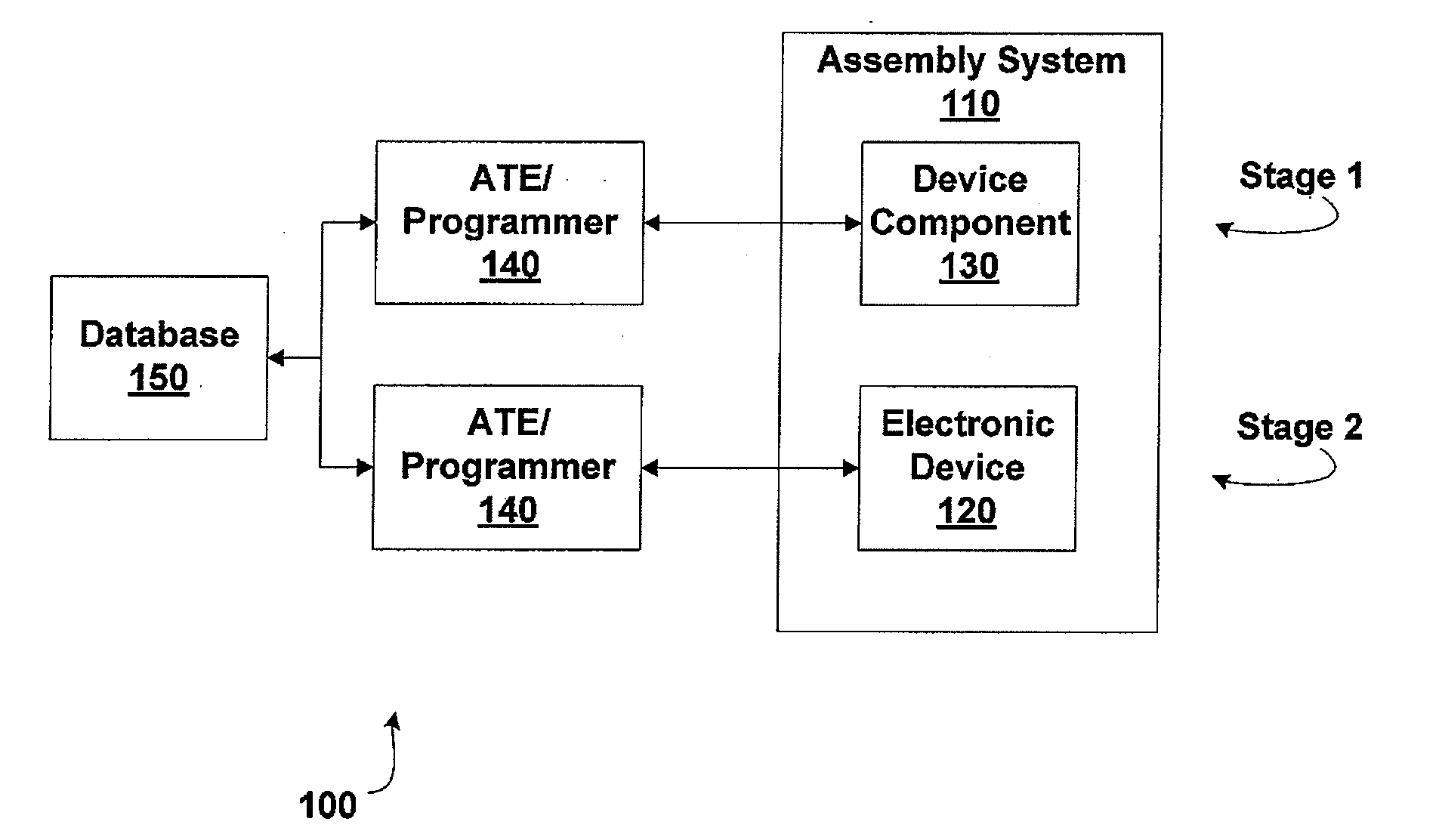
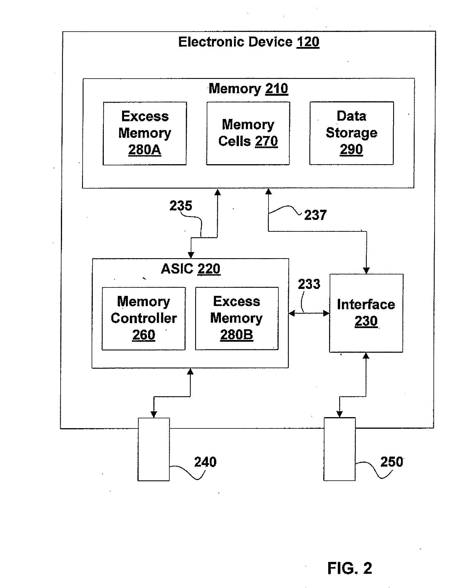
[0040] Various embodiments of the invention include systems for and methods of manufacturing an electronic device having a plurality of device components. The systems for manufacturing may include, for example, device components, assembly systems, data systems, programming equipment and test equipment. The assembly systems are configured for incorporating the device components into electronic device packaging to form the electronic device.

[0041] The assembled electronic device includes an excess (e.g., a redundancy) of one or more circuit types. For example, in some embodiments, the device components include an excess of memory circuits. As is described further herein, the excess of memory circuits are used as replacements for any memory circuits determined to be defective using the test equipment. The excess memory circuits are optionally disposed within a different device component than the defective circuits they are configurable to replace. In alternative embodiments, the exces...


PUM


Abstract

Disclosed are systems and methods of producing electronic devices including an auxiliary circuit mounted on another, underlying, circuit at the wafer level. The auxiliary circuit is electrically connected to the underlying circuit via micro-scale interconnects. The systems are capable of testing the auxiliary circuit and / or interconnects using an interface within the underlying circuit. For example, the auxiliary circuit may be tested although it is mounted such that the interconnects are hidden, i.e., inaccessible for testing purposes after assembly using conventional testing systems and methods. The systems and methods further allow for including excess circuits and / or excess interconnects that can be reconfigured to replace parts of the auxiliary circuit and / or micro-scale interconnects found defective during testing.

Description

CROSS-REFERENCE TO RELATED APPLICATIONS [0001] This application is a continuation-in-part of co-pending U.S. patent application Ser. No. 11 / 258,484, filed on Oct. 24, 2005, entitled “Component Testing and Recovery,” which is related to co-pending U.S. patent application Ser. No. 11 / 108,385, filed on Apr. 18, 2005, entitled “Bonding pads for testing of a semiconductor device,” which is a divisional of U.S. Pat. No. 6,882,171 filed on Jun. 27, 2003 and entitled “Bonding pads for testing of a semiconductor device,” which is a continuation-in-part of U.S. Pat. No. 6,812,726, filed on Nov. 27, 2002, entitled “Entering test mode and accessing of a packaged semiconductor device.”[0002] This application is also related to co-pending U.S. patent application Ser. No. 10 / 679,673, filed on Oct. 3, 2003, entitled “Set up for a first integrated circuit chip to allow for testing of a co-packaged second integrated circuit chip,” and to U.S. patent application Ser. No. 11 / 207,665, filed on Aug. 18, ...

Claims


Application Information

Patent Timeline
Patent Type & Authority Applications(United States)
IPC IPC(8): G01R31/28
CPCG11C29/1201G11C29/48G11C29/72
Inventor ONG, ADRIAN E.
Owner RAMBUS INC
Why Eureka
Try Eureka