
Patsnap Eureka
For R&D, Patsnap Eureka makes reading and utilizing patents & technical documents easy.
Patsnap Eureka AIR
Designed for self-driven R&D workflows. Generate viable solutions, solve complex R&D challenges, empower your innovation with AI.

Patsnap Eureka Materials
Designed for material experts only. Revolutionize your material R&D, from search, analyze, to developing new materials.

TechResearch
Generate reliable direction feasibility study reports for your R&D in just a few steps.

TechSeek
Discover and master advanced knowledge NOW. Basics, ideas, possibilities, all at once.

TechMind
As an expert in R&D Theories, TechMind can generates customized viable solutions instantly.

TechRisk
Analyze your overall solution with one click, know your potential R&D risks in advance.

TechMonitor
Get weekly tech updates, stay abreast of the latest tech innovations and key insights.
Non-volatile semiconductor memory element and method of manufacturing the same, and semiconductor integrated circuit device including the non-volatile semiconductor memory element
- Summary
- Abstract
- Description
- Claims
- Application Information
AI Technical Summary
Benefits of technology
Problems solved by technology
Method used
Image

Examples
first embodiment
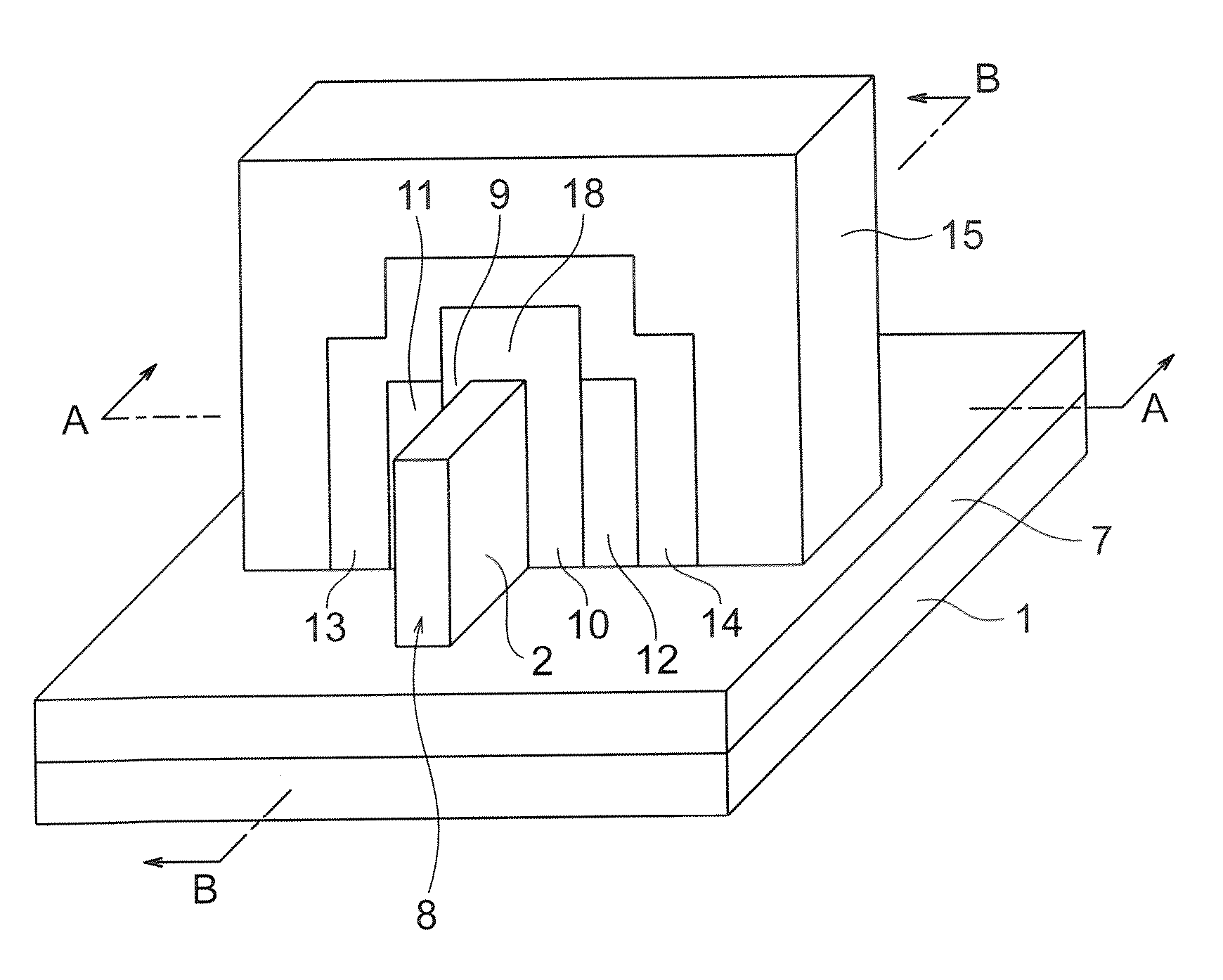
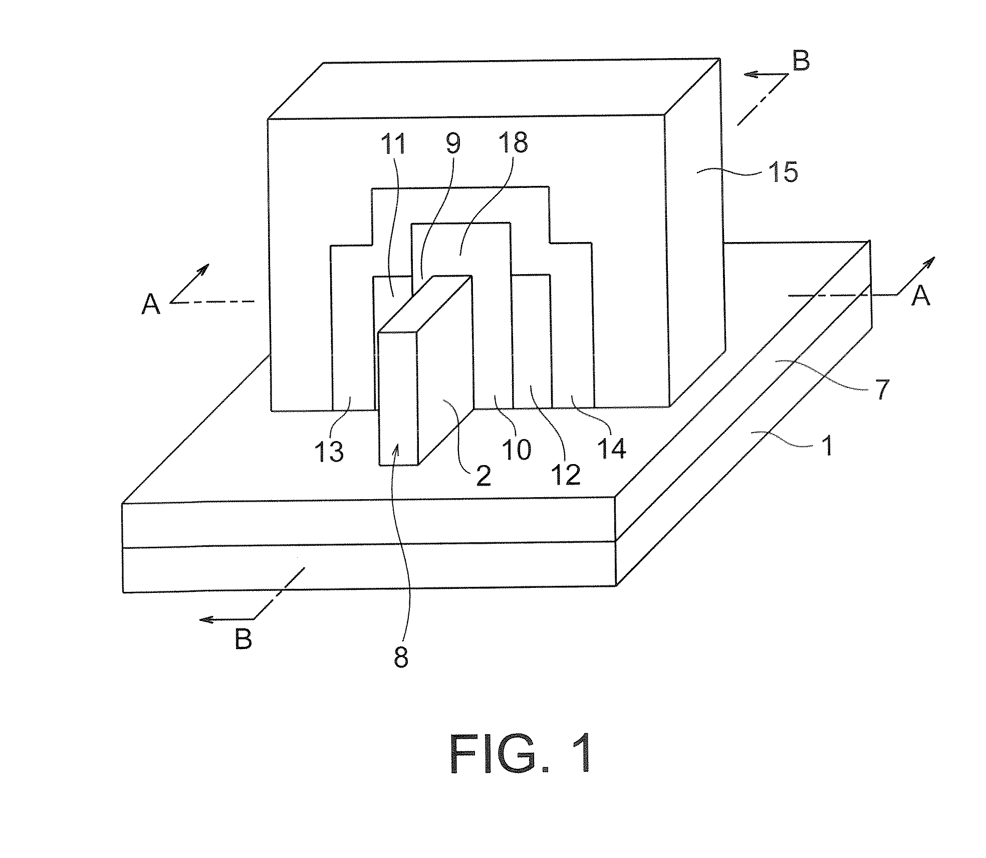
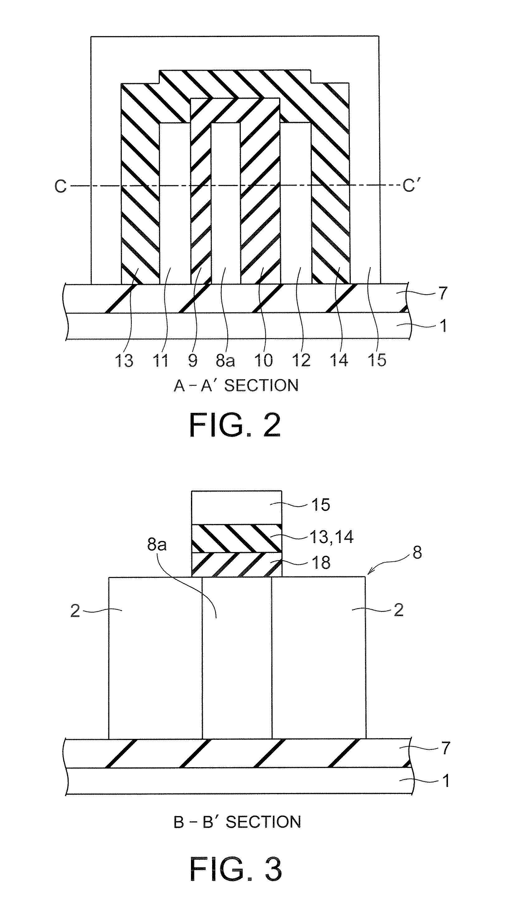
[0061]FIG. 1 is a perspective view of a non-volatile semiconductor memory element according to a first embodiment of the present invention. FIG. 2 is a cross-sectional view of the non-volatile semiconductor memory element, taken along the line A-A′ of FIG. 1. FIG. 3 is a cross-sectional view of the non-volatile semiconductor memory element, taken along the line B-B′ of FIG. 1. The non-volatile semiconductor memory element of this embodiment is formed on a SOI (Silicon On Insulator) substrate. A plate-like semiconductor region 8 having a channel region 8a is provided on an embedded insulating film 7 formed on a supporting substrate 1. A first tunnel gate insulating film 9 is provided on one of the side faces of the semiconductor region 8, so as to cover the channel region 8a. A second tunnel gate insulating film 10 is provided on the other one of the side faces of the semiconductor region 8. The upper face of the channel region 8a is covered with a sidewall 18 made of silicon oxide. ...
second embodiment
[0113]FIG. 17 is a perspective view of a non-volatile semiconductor memory element according to a second embodiment of the present invention. The non-volatile semiconductor memory element of this embodiment is formed on a SOI substrate. A plate-like semiconductor region 8 having a channel region is provided on an embedded insulating film 7 formed on a supporting semiconductor substrate 1. An insulating film 18 made of silicon oxide is provided on the top face of the semiconductor region 8. A first ferroelectric insulating film 21 is provided on one of the side faces of the semiconductor region 8 and the insulating film 18, so as to cover the channel region. A second ferroelectric insulating film 22 is provided on the other one of the side faces of the semiconductor region 8 and the insulating film 18, so as to cover the channel region. A gate electrode 23 is provided so as to cover the semiconductor region 8, the insulating film 18, and the first and second ferroelectric insulating ...
third embodiment
[0133] Referring now to FIG. 25, a semiconductor integrated circuit device according to a third embodiment of the present invention is described. FIG. 25 is a circuit diagram of the semiconductor integrated circuit device of this embodiment. The semiconductor integrated circuit device of this embodiment is a non-volatile semiconductor memory in which non-volatile semiconductor memory elements of either the first or second embodiment are arranged in a lattice-point form. The non-volatile semiconductor memory elements (hereinafter referred to simply as the memory elements) of either the first or second embodiment are represented by Tri,j in FIG. 25 (1≦i≦M, 1≦j≦N).
[0134] The memory elements located in the same row have the plate-like semiconductor regions connected to one another. The memory elements located in the same column have the control gate electrodes or the gate electrodes (hereinafter collectively referred to as the “control gate electrodes”) connected to one another. The pl...
PUM
 Abstract
Description
Claims
Application Information
 - R&D Engineer
- R&D Manager
- IP Professional
- Industry Leading Data Capabilities
- Powerful AI technology
- Patent DNA Extraction
Browse by: Latest US Patents, China's latest patents, Technical Efficacy Thesaurus, Application Domain, Technology Topic, Popular Technical Reports.
© 2024 PatSnap. All rights reserved.Legal|Privacy policy|Modern Slavery Act Transparency Statement|Sitemap|About US| Contact US: help@patsnap.com