Image display device

Inactive Publication Date: 2007-05-24
HITACHI DISPLAYS
View PDF2 Cites 5 Cited by
  • Summary
  • Abstract
  • Description
  • Claims
  • Application Information

AI Technical Summary

Benefits of technology

[0029] At a portion of the sealing region formed between the frame body and the back substrate, a length of a sealing region portion arranged inside the panel differs from a length of the sealing region portion arranged outside the panel. By setting the line-penetrating-direction length of an evacuated region side (inside) of the sealing region larger than the line-penetrating-direction length of an atmospheric pressure side of the sealing region, it is possible to ensure an engaging space between a terminal and an external circuit and, at the same time, it is possible to prevent the leaking of vacuum from being generated thus obtaining the highly reliable image display device which can possess a prolonged lifetime.
[0030] The first lines and the second lines differ from each other in thickness inside the sealing region and hence, it is possible to select a size of the sealing region corresponding to a line film thickness and thus obtaining the highly reliable image display device which can prevent the leaking of vacuum from being generated and can possess a prolonged lifetime.
[0031] At least either one of the first lines and the second lines have line portions thereof which are arranged inside the panel and in the sealing region formed into the stacked structure and hence, it is possible to realize thic

Problems solved by technology

According to such a large quantity of flow of the current, there arises a drawback that a voltage drop is generated along the scanning signal lines.
However, when the film thickness is increased, a stress in the line is increased thus giving rise to a drawback that the line is easily peeled off from the back substrate.
This drawback also arises with

Method used


Image

  • Image display device
  • Image display device
  • Image display device

Examples


embodiment 1

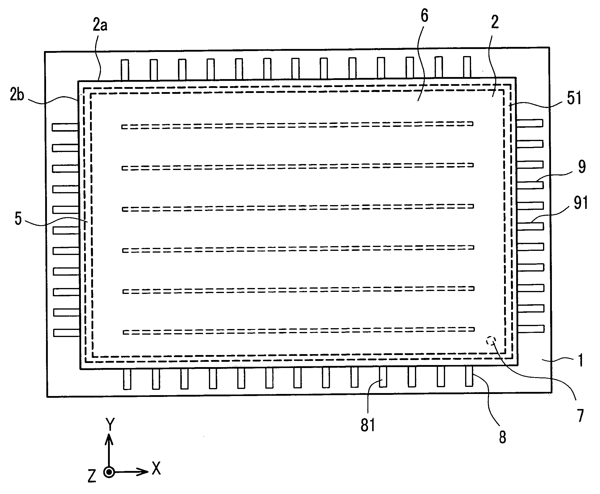
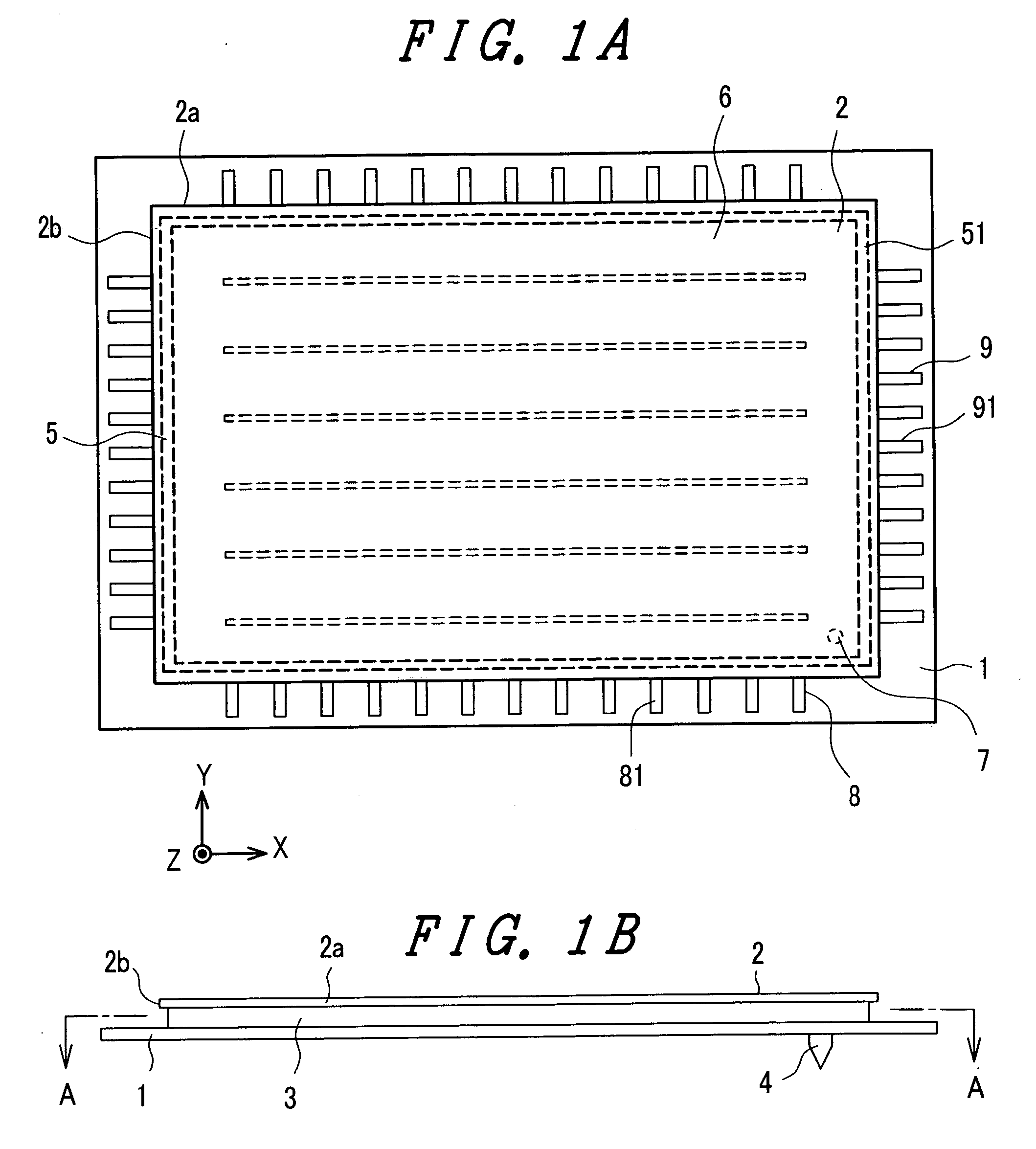
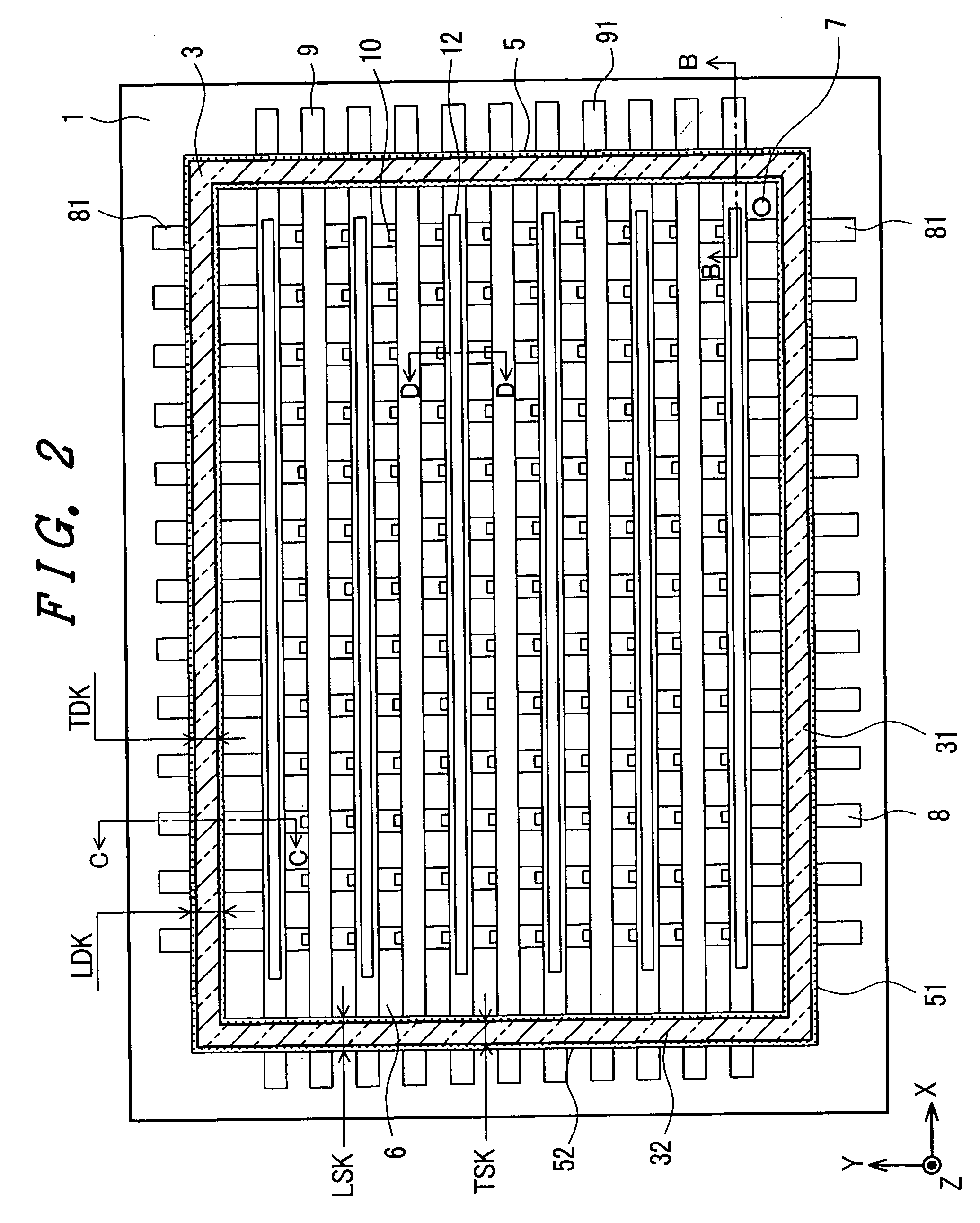
[0047]FIG. 1A to FIG. 5 are views for explaining one embodiment of an image display device according to the present invention. FIG. 1A is a plan view as viewed from a face substrate side, FIG. 1B is a side view of FIG. 1A, FIG. 2 is a schematic plan view taken along a line A-A in FIG. 1B, FIG. 3 is a schematic cross-sectional view of a back substrate taken along a line B-B in FIG. 2 and a schematic cross-sectional view of a portion of the face substrate which corresponds to the back substrate, FIG. 4 is a schematic cross-sectional view of a back substrate taken along a line C-C in FIG. 2 and a schematic cross-sectional view of a portion of the face substrate which corresponds to the back substrate, and FIG. 5 is a schematic cross-sectional view of a back substrate taken along a line D-D in FIG. 2 and a schematic cross-sectional view of a portion of the face substrate corresponding to the back substrate.

[0048] In these FIG. 1A to FIG. 5, numeral 1 indicates a back substrate and nume...

embodiment 2

[0068]FIG. 6 is a schematic cross-sectional view of another embodiment of the image display device of the present invention and corresponds to FIG. 4, wherein parts which are identical with the parts described in FIG. 6 are given the same symbols. In FIG. 6, as described above, the frame body 3 is formed of, for example, a frit glass sintered body, a glass plate or the like, and the frame body 3 is formed by a single body or by a combination of a plurality of members and is formed in a substantially rectangular frame shape.

[0069] In the frame body 3, a thickness TDK of a pair of frame body members 31 which are arranged on the long side of the substantially-rectangular-shaped frame body 3 and a thickness TSK of a pair of frame body members 32 which are arranged on short side of the substantially-rectangular-shaped frame body 3 are set to a same size. That is, by establishing the relationship TDK=TSK, the thickness of the frame body 3 is set to the substantially same size over the wh...

embodiment 3

[0072]FIG. 7 is a schematic cross-sectional view of still another embodiment of the image display device of the present invention and corresponds to FIG. 3 described above, wherein parts which are identical with the parts described in FIG. 7 are given the same symbols. In FIG. 7, the center of the penetrating direction length of the second sealing region 52 into which the scanning lines 9 hermetically penetrate is offset from the center of the thickness direction of the frame body 3.

[0073] In the above-mentioned constitution, the penetrating direction length LSK of the second sealing region 52 is set to a size which is obtained by synthesizing three portions, that is, a length LSKI which is arranged inside the panel, a thickness TSK of the frame body 3 and a length LSKO which is arranged outside the frame body 3 and, at the same time, the length LSKI which is arranged inside the panel is set larger than the length LSKO which is arranged outside the frame body 3. Further, other cons...


PUM


Abstract

An image display device is constituted such that a back substrate on which image signal lines, scanning signal lines and electron sources are arranged and a face substrate which has phosphor layers are hermetically sealed to each other by way of a frame body using a sealing material, and the inside of the image display device is formed into a vacuum. A length LSK of a second sealing region into which scanning signal lines hermetically penetrate is set larger than a length LDK of a first sealing region into which thin-film image signal lines hermetically penetrate and hence, it is possible to suppress the decrease of the degree of vacuum.

Description

BACKGROUND OF THE INVENTION [0001] 1. Field of the Invention [0002] The present invention relates to a planar image display device which makes use of emission of electrons into vacuum formed between a face substrate and a back substrate. [0003] 2. Description of the Related Art [0004] A color cathode ray tube has been popularly used conventionally as an excellent display device which exhibits high brightness and high definition. However, along with the realization of high image quality of recent information processing device and television broadcasting, there has been a strong demand for a planar image display device (flat panel display, FPD) which is light-weighted and requires a small space for installation while ensuring the excellent properties such as high brightness and high definition. [0005] As typical examples of such a planar image display device, a liquid crystal display device, a plasma display device or the like has been put into practice. Further, particularly with res...

Claims


Application Information

Patent Timeline
IPC IPC(8): H01J63/04H01J1/62
CPCH01J29/87H01J29/90H01J31/127
Inventor KIJIMA, YUUICHIKANEKO, YOSHIYUKIKATO, KENJIOROKU, NORIYUKISASAMOTO, TOSHIO
Owner HITACHI DISPLAYS
Why Eureka
Try Eureka