Plasma display apparatus and method of manufacturing the same

Inactive Publication Date: 2007-05-24
SAMSUNG SDI CO LTD
View PDF3 Cites 8 Cited by
  • Summary
  • Abstract
  • Description
  • Claims
  • Application Information

AI Technical Summary

Benefits of technology

[0010] The present embodiments provide a plasma display apparatus having an improved structure so as to increase luminescence efficiency and uniformity and a method of manufacturing the plasma display apparatus.
[0013] According to another aspect of the present embodiments, there is provided a plasma display apparatus, comprising: a front substrate and a rear substrate facing each other; a plurality of first and second sustain electrodes formed on the front substrate and spaced apart from each other; first and second electron emitting layers formed on the first and second sustain electrodes, respectively, emitting electrons received from the first and second sustain electrodes; and a dielectric layer covering the first and second electron emitting layers, having a window exposing an upper face of the first and second electron emitting layers, and having a structure in which the closer the first and second electron emitting layers are to a gap between the first and second sustain electrodes, the thinner the window becomes.
[0014] The first and second electron emitting layers may be formed of an OPPS or an OPAS. The first and second sustain electrode are formed of one selected from a group consisting of ITO, Al, and Ag. A density of electrons emitted from the first and second electron emitting layers may be relatively varied according to the width of the window. The closer the first and second electron emitting layers are to the gap between the first and second sustain electrodes, the lower the density of electrons emitted from the first and second electron emitting layers is. The farther the first and second electron emitting layers are from the gap between the first and second sustain electrodes, the higher the density of electrons emitted from the first and second electron emitting layers is.

Problems solved by technology

However, the density of electron emission contributing to the discharge is not constant in the unit discharge cells, thus reducing luminescence uniformity of the conventional PDP illustrated in FIG. 1.
As a result, the conventional PDP has a high discharge voltage and a low discharge or luminescence efficiency.

Method used


Image

  • Plasma display apparatus and method of manufacturing the same
  • Plasma display apparatus and method of manufacturing the same
  • Plasma display apparatus and method of manufacturing the same

Examples


Embodiment Construction

[0027] The present embodiments will now be described more fully with reference to the accompanying drawings, in which exemplary embodiments are shown. In the drawings, the thickness of layers and regions are exaggerated for clarity.

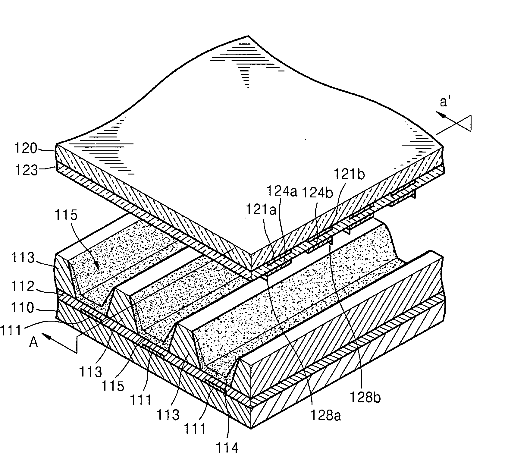
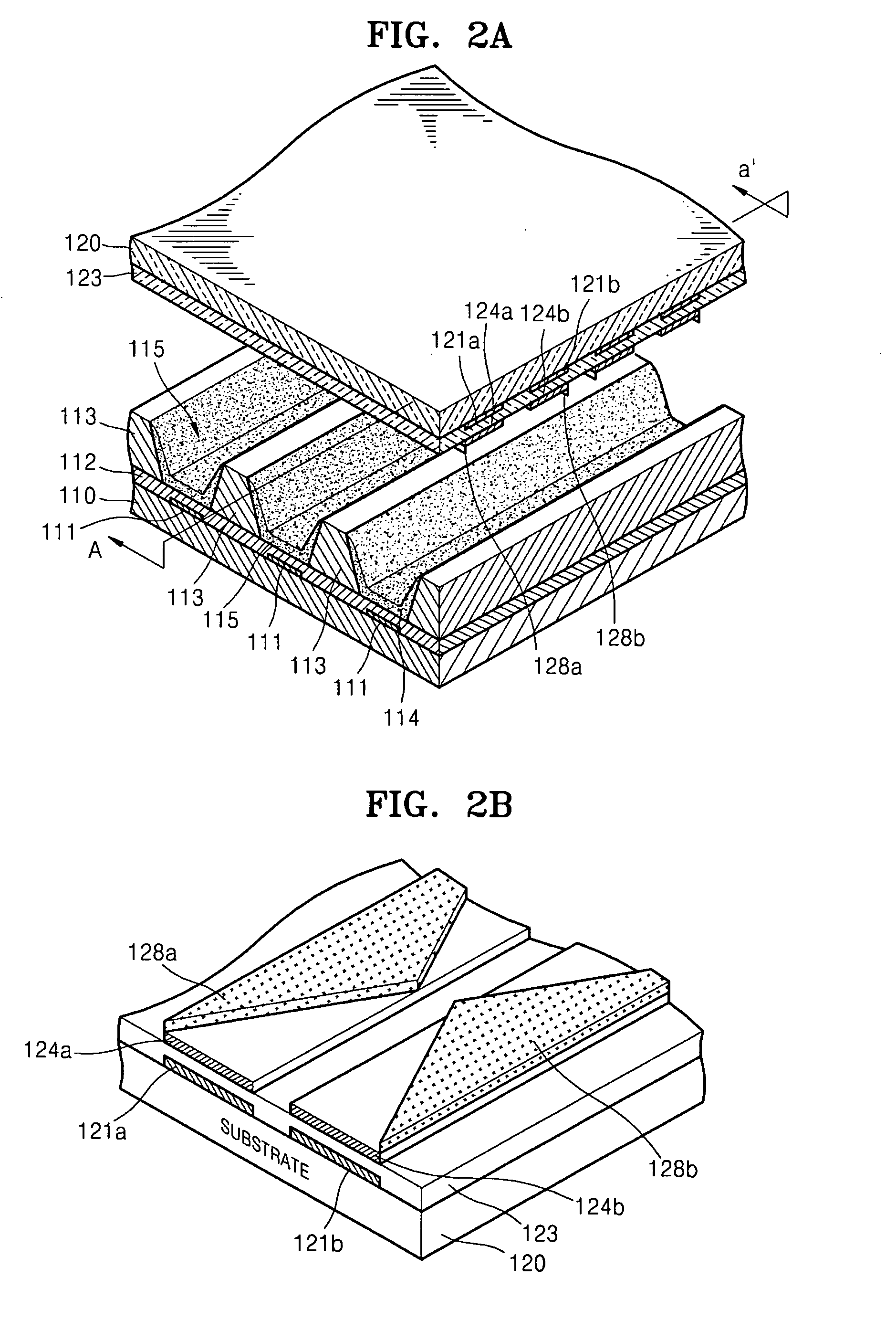
[0028]FIG. 2A is an exploded perspective view of a plasma display apparatus according to an embodiment. FIG. 2B is a cross-sectional view of the plasma display apparatus of FIG. 2A taken along a line A-a′ in FIG. 2A according to an embodiment. A plasma display panel (PDP) is realized as an example of the plasma display apparatus according to the current embodiment.

[0029] Referring to FIGS. 2A and 2B, the plasma display apparatus according to the current embodiment includes a front substrate 120 and a rear substrate 110 which face each other, and a plurality of barrier ribs 113 interposed between the front substrate 120 and the rear substrate 110, forming discharge spaces 115 filled with a discharge gas such as, for example, Neon Ne or Xenon Xe. The barr...


PUM


Abstract

A plasma display apparatus having an improved structure so as to increase luminescence efficiency and uniformity and a method of manufacturing the display apparatus are provided. The display apparatus includes: a front substrate and a rear substrate facing each other; a plurality of first and second sustain electrodes formed on the front substrate and spaced apart from each other; and first and second electron emitting layers formed on the first and second sustain electrodes, respectively, emitting electrons received from the first and second sustain electrodes, and having a structure in which their thickness decreases as they approach a gap between the first and second sustain electrodes.

Description

CROSS-REFERENCE TO RELATED PATENT APPLICATION [0001] This application claims the benefit of Korean Patent Application No. 10-2005-0112239, filed on Nov. 23, 2005 in the Korean Intellectual Property Office, the disclosure of which is incorporated herein in its entirety by reference. BACKGROUND OF THE INVENTION [0002] 1. Field of the Invention [0003] The present embodiments relate to a plasma display apparatus, and more particularly, to a plasma display apparatus having an improved structure so as to increase luminescence efficiency and uniformity and a method of manufacturing the plasma display apparatus. [0004] 2. Description of the Related Art [0005] Plasma display panels (PDPs) form images using electrical discharge, have good brightness characteristics and a wide viewing angle, etc., leading to an increase in the use of PDPs recently. PDPs display images using visible light emitted through a process of exciting a phosphor material with ultraviolet rays generated from a discharge ...

Claims


Application Information

Patent Timeline
IPC IPC(8): H01J17/49H01J9/02H01J11/12H01J11/22H01J11/24H01J11/26H01J11/30H01J11/34H01J11/38H01J11/40H01J11/44
CPCH01J9/02H01J11/28H01J11/40H01J2211/225H01J11/22H01J11/34
Inventor PARK, HYOUNG-BINSON, SEUNG-HYUNJANG, SANG-HUNKIM, GI-YOUNGKIM, SUNG-SOOLEE, HO-NYEON
Owner SAMSUNG SDI CO LTD
Why Eureka
Try Eureka