Multilayer printed wiring board and method for producing the same

a printing method and wiring board technology, applied in the direction of printed circuit manufacturing, printed circuit aspects, non-metallic protective coating applications, etc., can solve the problems of reducing the service life of the wire, so as to improve the work efficiency and reduce the cost. , the effect of dimensional precision and wiring density

Inactive Publication Date: 2007-05-24
SHARP KK
View PDF5 Cites 12 Cited by
  • Summary
  • Abstract
  • Description
  • Claims
  • Application Information

AI Technical Summary

Benefits of technology

[0099] As described above, according to the present invention, an effect is exhibited in which because a covering layer is formed after forming an inner layer and an outer layer, and the covering layer is shared by a flexible portion and at least part of a hard portion, the covering layer can be configured as a single body from the flexible portion to the hard portion over the border of the flexible portion and the hard portion. Thus, additional, resin processing for the sake of reinforcement at the border of the a flexible portion Af (see embodiments below) and a hard portion As (see embodiments below) used in the conventional technology is made unnecessary, and along with this, a multilayer printed wiring board is possible in which flexibility is provided, and in which structural and strength-wise discontinuity is greatly improved over the conventional methods.
[0100] Also, according to the present invention, an effect is exhibited in which layer pressing of the covering layer, which is a heat layering process, is not performed in the processing after inner layer formation and before outer layer formation, so work efficiency can be improved, and it is possible to ...

Problems solved by technology

This is accompanied by the appearance of various problems, such as problems of unevenness in the vicinity of the border between the flexible portion and the hard portion, problems in surface treatment for an exposed portion of the flexible portion, and the necessity of process simplification.
As described above, the hard base material 120 is formed with a glass epoxy substrate or the like and is thus brittle, so it is comparatively fragile, and can be torn away.
That is, there are the problems that (1) manufacturability is diminished because processing is difficult and long, and (2) after surface treatment of the flexible portion there is heat processing and wet processing such as layer pressing of the hard portion or outer layer circuit pattern formation, and further, the flexible portion is placed in a sealed environment by the hard base material, and thus a phenomenon occurs in which the flexible portion on which predetermined surface treatment has been performed is contaminated by gas or adhesive flow generated during processing, various impregnated processing agents, water, or the like.
However, because a large difference in the thickness of the flexible portion and the hard portion is produced, unified processing of the flexible portion (inner layer circuit pattern) and the outer layer circuit pattern, as stated next, is difficult and could not be realized in the conventional technology.
Accordingly, in the vicinity of the border of the hard portion and the flexible portion, because there is a large height difference, the polishing brush does not make good contact, conversely, there is the problem that processing with the polishing brush damages the corners of the hard portion.
Also, when performing plating processing, formation of a plating resist or the like is necessary, but in the vicinity of the border of the flexible portion and the hard portion a portion is produced in which the resist does not fit closely, so there is the problem that processing such as plating processing cannot be performed normally.
Also, when providing a thermocompression pressing process in order to layer and bond the covering layer (coverlay) in the next processing after processing of the flexible base material, the dimensions of the flexible base material change, and this is disadvantageous when manufacturing a high-precision, high-density multilayer printed wiring board.
On the other hand, methods have been proposed in which an ink covering layer is executed in the flexible portion in order to lower heat and pressure stress, but there is the problem that the flexibility properties of the flexible portion are poor compared to the covering layer of the insulating resin film.
Further, in the hard portion and the flexible portion, because there is a large difference in materials and structure (for example, such as a height difference), there is the problem that discontinuity in strength/structure causes damage to the conductor of the flexible portion or the hard ...

Method used


Image

  • Multilayer printed wiring board and method for producing the same
  • Multilayer printed wiring board and method for producing the same
  • Multilayer printed wiring board and method for producing the same

Examples


embodiment 1

[0120] FIGS. 1 to 7 are explanatory diagrams for explaining the state of a multilayer printed wiring board in each production process for a multilayer printed wiring board according to Embodiment 1 of the present invention.

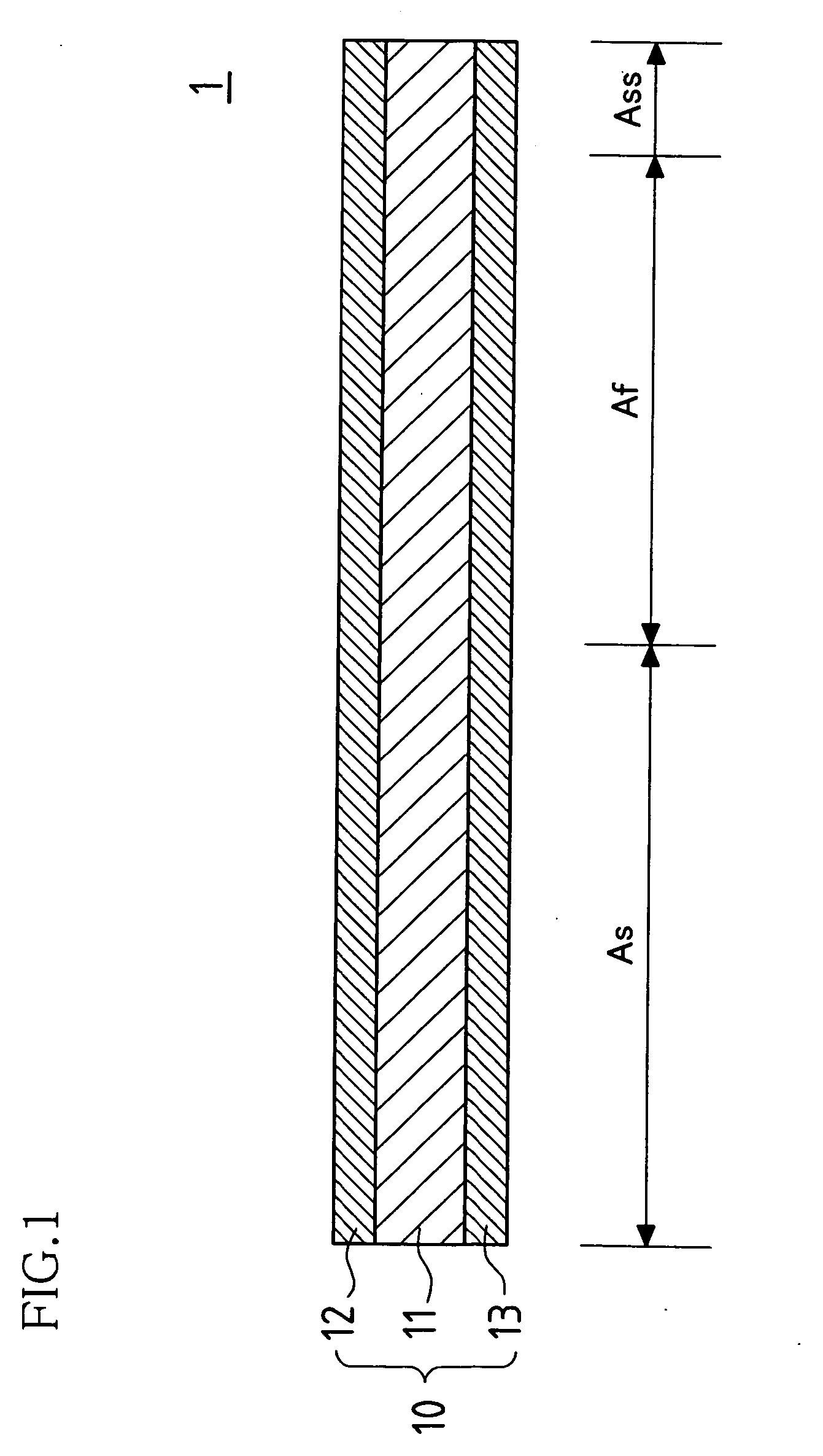
[0121]FIG. 1 is a cross-sectional diagram that shows a cross-section of a flexible base material that constitutes an inner layer and a flexible portion, in a multilayer printed wiring board according to Embodiment 1 of the present invention.

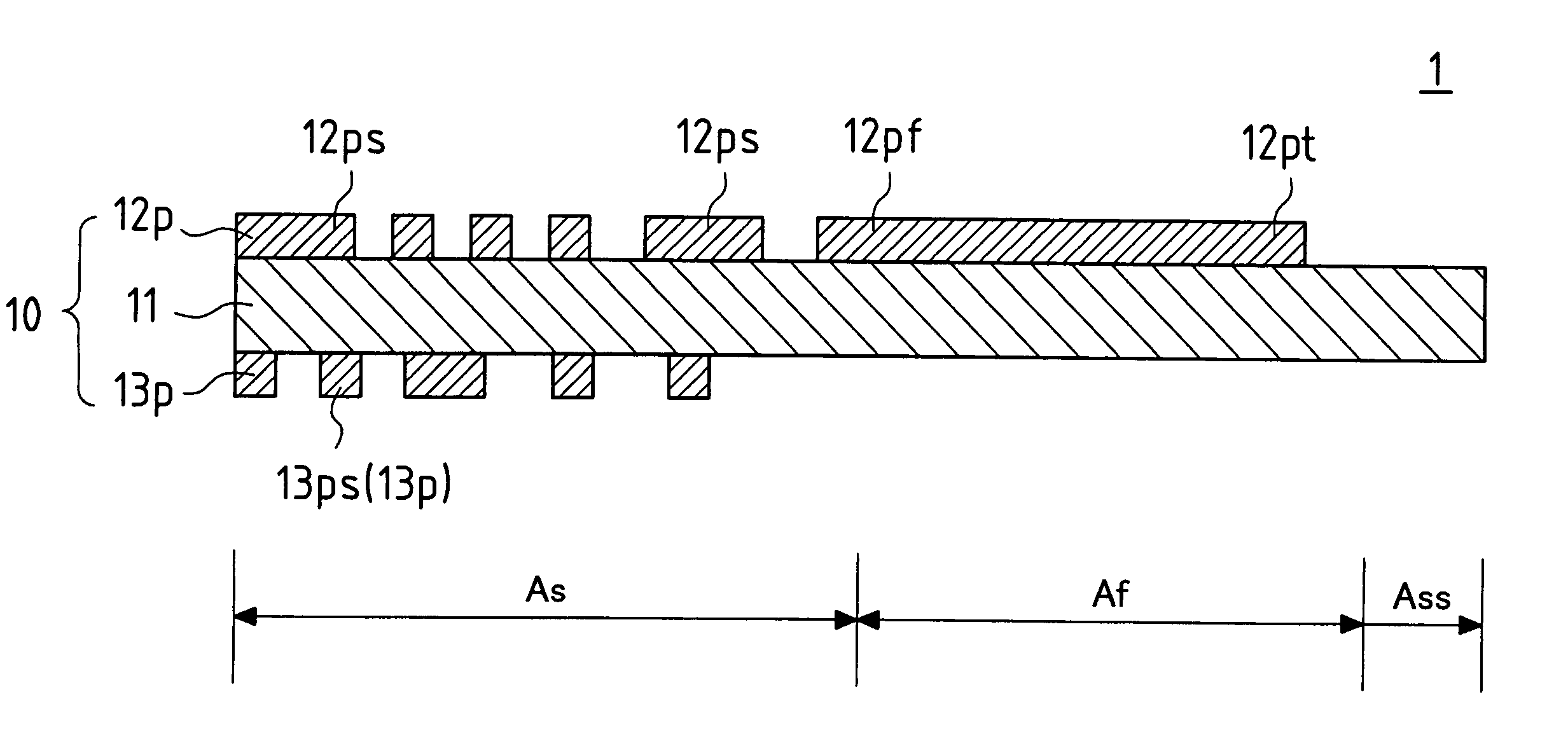
[0122] A flexible base material 10 that constitutes an inner layer and a flexible portion Af of a multilayer printed wiring board 1 is provided with an insulation layer 11 and conductor layers 12 and 13 that have been layered on both faces of the insulation layer 11. Below, this is referred to as the multilayer printed wiring board 1 even in the midst of processing.

[0123] As the flexible base material 10, two-sided flexible wiring board material that is ordinarily commercially available can be used. The insulation layer 11 i...

embodiment 2

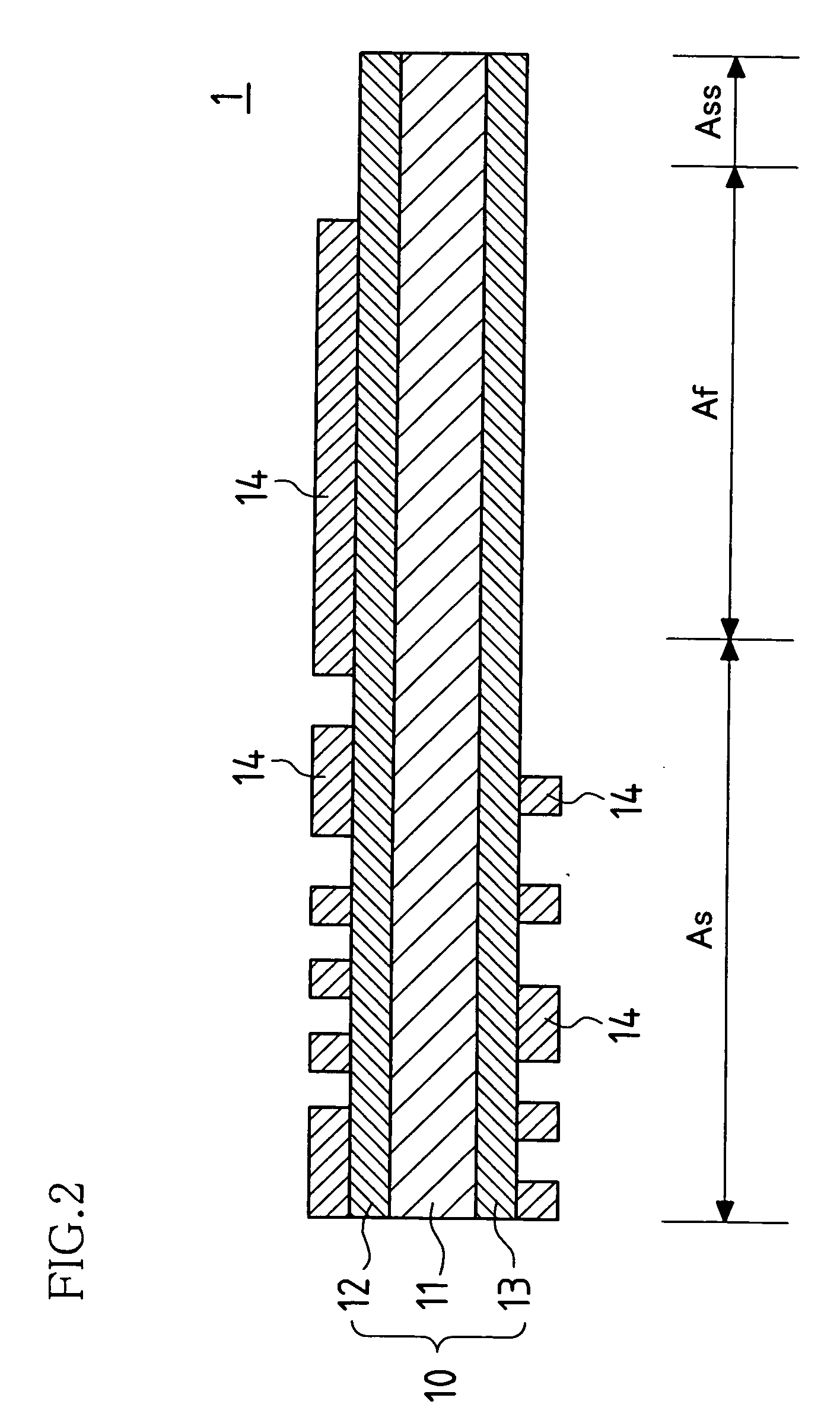
[0165]FIG. 8 is a cross-sectional diagram that shows a cross-section of a state in which a covering layer has been formed, in a multilayer printed wiring board according to Embodiment 2 of the present invention. The same configurations as in Embodiment 1 have the same reference numerals, and a detailed description thereof is omitted here.

[0166] The present embodiment is nearly the same as Embodiment 1, but here the configuration of the covering layers 30 and 31 in Embodiment 1 is modified.

[0167] In the present embodiment, instead of the covering layers 30 and 31 formed in Embodiment 1, covering layers 32, 33, and 34 are formed. That is, corresponding to the covering layer 30, a first covering layer 32 that continuously covers a partial region of the hard base material 20 and the flexible base material 10, and a second covering layer 33 that covers a region other than the partial region of the hard base material 20, are formed, and corresponding to the covering layer 31, a covering...

embodiment 3

[0169] In the process of layering the hard base material 20 according to Embodiment 1, the hard base material 20 of the region that corresponds to the flexible portion Af and the flexible base material 10, although the adhesive layers 15 and 16 are not present, is fitted very well with pressure and heat when layering.

[0170] Accordingly, in order to peel away the hard base material 20 of the region that corresponds to the flexible portion Af without deforming or damaging the flexible portion Af, careful work is necessary, and defects easily occur. Also, because processing work is performed on a one-by-one basis for each multilayer printed wiring board 1, work efficiency also is very poor. As described below, in the present embodiment such problems do not occur.

[0171]FIG. 9 is a cross-sectional diagram that shows a cross-section of a state in which a hard base material that constitutes an outer layer has been formed outside of an inner layer, in a multilayer printed wiring board acc...


PUM


Abstract

A multilayer printed wiring board includes a flexible portion that is constituted from a flexible base material in which an inner layer circuit pattern has been formed, and a hard portion that is constituted from a hard base material that is layered on a portion of the flexible base material via an adhesive layer and in which an outer layer circuit pattern has been formed. The border of the flexible portion and the hard portion is covered by a covering layer that continuously covers the flexible base material and the hard base material, with an exposed portion of the inner layer circuit pattern being exposed. A plating layer is formed by performing surface treatment (plating) for the exposed portion and the outer layer circuit pattern.

Description

BACKGROUND OF THE INVENTION [0001] This application claims priority under 35 U.S.C. § 119(a) on Japanese Patent Application No. 2005-334421 filed in Japan on Nov. 18, 2005, the entire contents of which are hereby incorporated by reference. [0002] The present invention relates to a printed wiring board for an electronic device that is used for implementation of an electronic component, and more specifically to a multilayer printed wiring board in which a conductor layer pattern of two or more layers is formed, and that has a flexible portion and a hard portion. [0003] A multilayer printed wiring board that has a flexible portion and a hard portion is commonly referred to as a “flex-rigid wiring board” or a “ multilayer flexible wiring board”, and is often used along with reductions in size, increasing precision, and compounding of an electronic device. This is accompanied by the appearance of various problems, such as problems of unevenness in the vicinity of the border between the f...

Claims


Application Information

Patent Timeline
IPC IPC(8): H01L21/00H01L23/02
CPCH05K3/064H05K3/243H05K3/28H05K3/4652H05K3/4688H05K3/4691H05K2201/0187
Inventor UENO, YUKIHIROTAKAMOTO, YUHJI
Owner SHARP KK
Why Eureka
Try Eureka