Switching power supply and semiconductor device used therefor

a technology of switching power supply and semiconductor device, which is applied in the direction of power conversion system, dc-dc conversion, electrical apparatus, etc., can solve the problems of difficult to downsize no countermeasures have been taken to reduce the and the difficulty of downsizing the switching power supply. to achieve the effect of reducing the size and noise of the switching power supply

Active Publication Date: 2007-05-31
COLLABO INNOVATIONS INC
View PDF2 Cites 70 Cited by
  • Summary
  • Abstract
  • Description
  • Claims
  • Application Information

AI Technical Summary

Benefits of technology

[0013] Therefore, in order to cope with the above-stated conventional problems, it is an object of the present invention to provide a switching power supply capable of reducing the size as well as the noise of the switching power supply.

Problems solved by technology

The above-stated conventional switching power supply requires an output voltage detection circuit that is connected with the secondary side in order to detect an output voltage and feed back the same to a control circuit, which makes it difficult to downsize a switching power supply.
Especially when the primary side and the secondary side are to be separated electrically using a photocoupler, it is difficult to downsize the switching power supply.
However, no countermeasures have been taken for reducing a switching noise.
To cope with this, the size of the switching transformer 101 will increase, which makes it difficult to downsize a switching power supply.

Method used


Image

  • Switching power supply and semiconductor device used therefor
  • Switching power supply and semiconductor device used therefor
  • Switching power supply and semiconductor device used therefor

Examples


embodiment 1

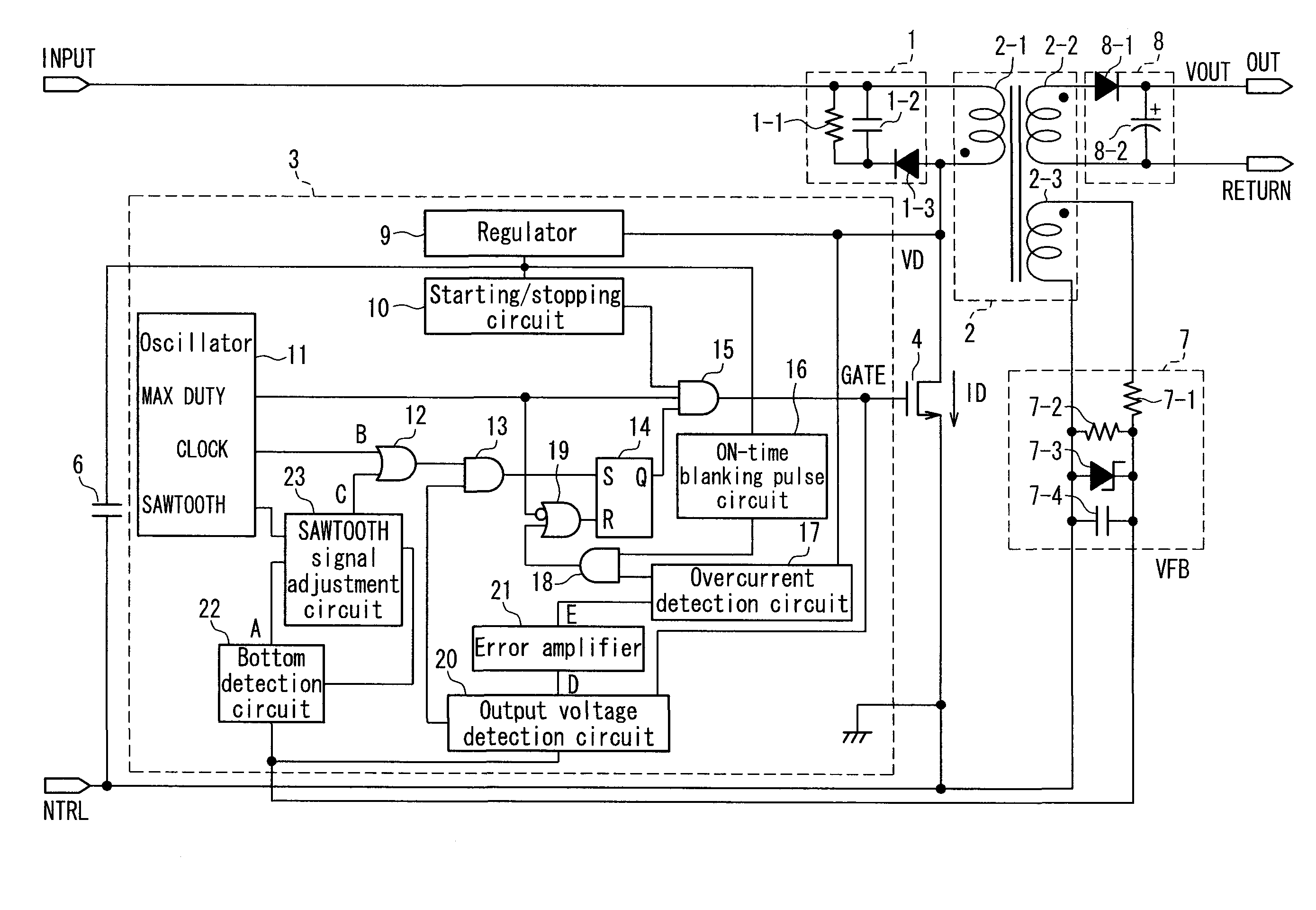
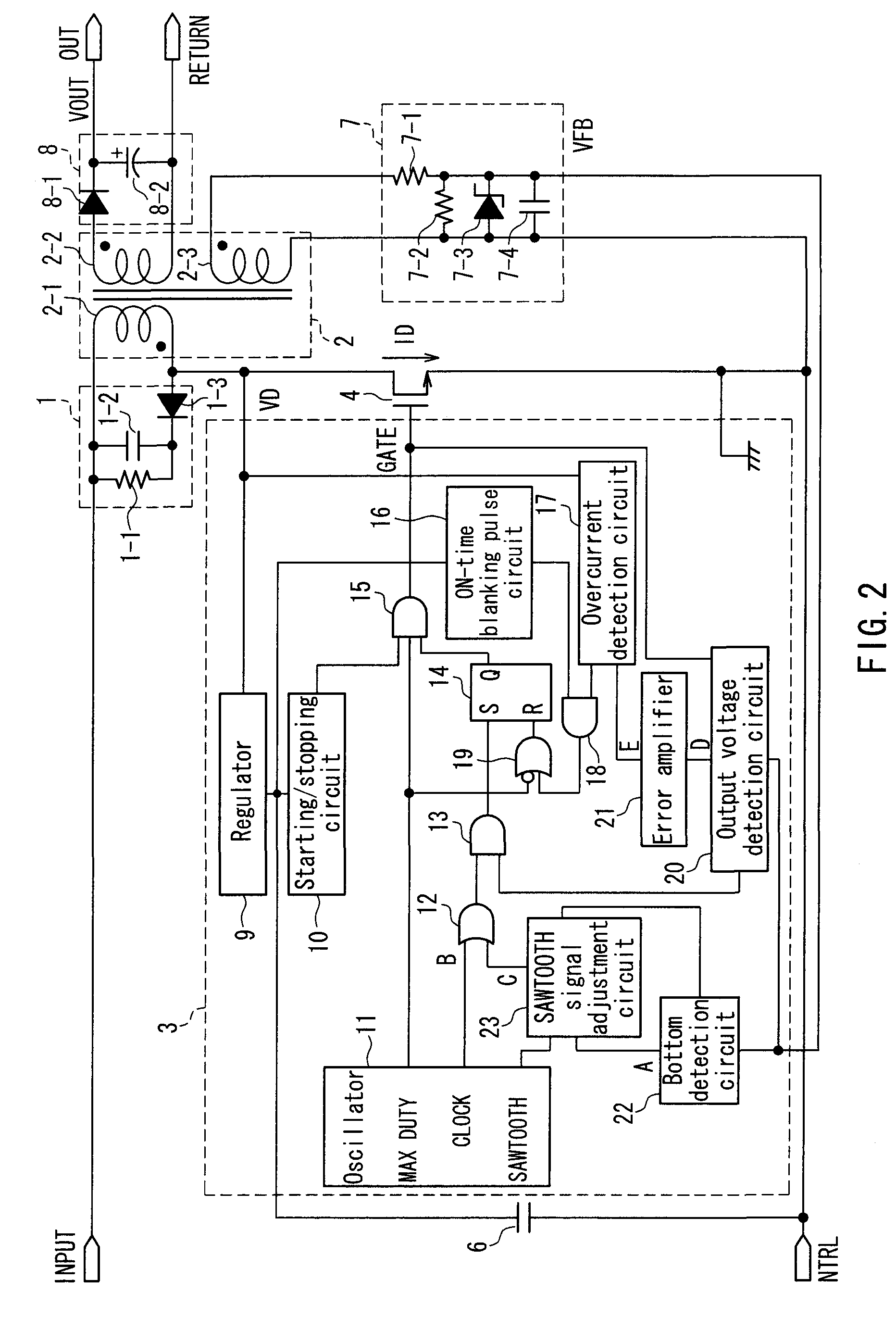
[0041]FIG. 2 is a circuit diagram of a switching power supply according to Embodiment 1 of the present invention. This switching power supply is provided with a switching transformer 2, a switching element 4 connected in series with a primary winding 2-1 of the switching transformer 2, a control circuit 3 that controls ON / OFF of the switching element 4, a rectifier / smoothing circuit 8 connected with one terminal of a secondary winding 2-2 of the switching transformer 2, a wave-shaping circuit 7 connected with an auxiliary winding 2-3 of the switching transformer 2 and the like. The control circuit 3 and the switching element 4 may be composed of individual semiconductor devices, or may be composed of a single semiconductor device.

[0042]FIG. 3 is a circuit diagram of a semiconductor device used for the switching power supply according to Embodiment 1 of the present invention. This semiconductor device 5 includes a single package with the control circuit 3 and the switching element 4...

embodiment 2

[0066]FIG. 7 is a circuit diagram of a semiconductor device used for a switching power supply according to Embodiment 2 of the present invention. The semiconductor device of the present embodiment includes an overvoltage detection circuit 24 and an overheat protection circuit 25 in addition to the semiconductor device of Embodiment 1 of FIG. 3, and the other configuration and the basic operation are the same as those of the semiconductor device of FIG. 3. Therefore, the switching power supply of the present embodiment can show the properties of the switching power supply according to Embodiment 1 of FIG. 2.

[0067] Since the switching power supply of the present embodiment additionally includes the overvoltage detection circuit 24 and the overheat protection circuit 25 in a control circuit 3 of the semiconductor device 5, the following effects can be obtained further.

[0068] The overvoltage detection circuit 24 detects the situation where an operating voltage VCC, which should be con...

embodiment 3

[0070]FIG. 8 is a circuit diagram of a semiconductor device used for a switching power supply according to Embodiment 3 of the present invention. The semiconductor device of the present embodiment includes a second switching element 26 and a resistor 27 in addition to the semiconductor device of Embodiment 1 of FIG. 3, and the other configuration and the basic operation are the same as those of the semiconductor device of FIG. 3. Therefore, the properties of the switching power supply according to Embodiment 1 of FIG. 2 can be obtained from the switching power supply of the present embodiment as well.

[0071] Since the switching power supply of the present embodiment additionally includes the second switching element 26 and the resistor 27, the following further effects can be obtained.

[0072] According to the semiconductor device of FIG. 3, the overcurrent detection circuit 17 detects the drain voltage VD at the time of the ON state of the switching element 4 to detect a current flo...


PUM


Abstract

A switching power supply capable of reducing the size as well as noise is provided. A switching element is connected in series with a primary winding of a transformer, a rectifier/smoothing circuit is connected with a secondary winding and a wave-shaping circuit is connected with an auxiliary winding. An operating voltage of a control circuit controlling ON/OFF of the switching element is supplied from a connection node between the primary winding of the transformer and the switching element. The control circuit includes: an output voltage detection circuit that obtains, from a voltage output from the wave-shaping circuit, a feedback voltage in proportion to a voltage output from the rectifier/smoothing circuit and generates a signal for PWM control of the switching element; and a bottom detection circuit that detects, from the voltage output from the wave-shaping circuit, a bottom level of a ringing voltage. The control circuit switches the switching element from OFF to ON in accordance with a signal output from an oscillator internal to the control circuit or a signal output from the bottom detection circuit.

Description

BACKGROUND OF THE INVENTION [0001] 1. Field of the Invention [0002] The present invention relates to a switching power supply and a semiconductor device used therefor. More particularly, the present invention relates to a novel control system that can reduce the size as well as noise of a switching power supply. [0003] 2. Description of Related Art [0004] In general, a switching power supply is provided with a switching transformer, a switching element connected in series with a primary winding of the switching transformer; a control circuit that controls ON / OFF of the switching element; a rectifier / smoothing circuit connected with a secondary winding of the switching transformer; and an output voltage detection circuit that feeds a detection voltage, changing in accordance with an output voltage of the rectifier / smoothing circuit, back to the control circuit (see JP 3480462B, for example). [0005]FIG. 1 is a circuit diagram showing an exemplary configuration of a conventional switch...

Claims


Application Information

Patent Timeline
Patent Type & Authority Applications(United States)
IPC IPC(8): H02H7/00
CPCH02M3/33507
Inventor HACHIYA, YOSHIAKI
Owner COLLABO INNOVATIONS INC
Why Eureka
Try Eureka